4 layer pcb design
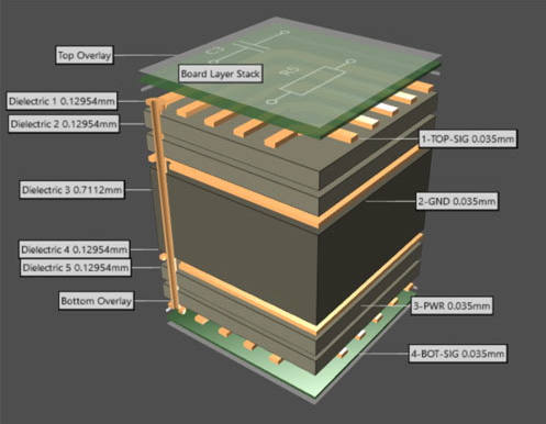
1.4 Layer Stacking
(1) What is Layer Stacking in PCB Design
In multilayer board design, three main types of layers are used. The layer types are signal layer, plane layer, and mixed layer.
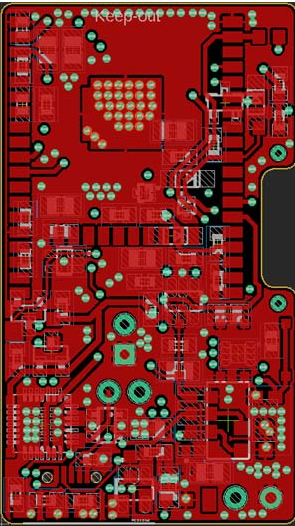
Signal layers consist of multiple types of signals. The following figure shows a perfect signal layer PCB, which has multiple types of signals and does not rely on special standards.
These are mainly low voltage, low current signals, mainly used to carry medium and high speed data lines.
This type of layer does not contain ground planes or power planes made by polygon pouring. There is a reason for this. In very high speed signals, the ground plane or power plane will cause impedance changes due to the accumulation of stray capacitance and stray inductance.
The following figure shows a signal layer where multiple signals are routed and components are placed
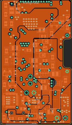
Plane layers are different. It does not contain any signals other than ground or power planes. This is useful for a number of reasons, mainly that the entire circuit has a good ground and power path. Solid copper is laid across the entire board, and by simply cutting the copper plane, separate segments can be created to provide different plane signals. Below is a good example where a plane layer is shown.
The next type of layer is a mixed layer, which uses signals and copper fill as one plane. This is the most commonly used layer type in two-layer and six-layer boards. It is sometimes also used in four-layer boards.
Multiple instances of this layer type can be seen on general PCB boards without obvious high-speed routing. The image given below shows an example of a mixed layer type.
(2). 4-layer stacking
For optimal performance, the layer assignment needs to be exactly as described below. The top and bottom layers can be used as signal layers, and the inner two layers can be used as power and ground, so that we can debug PCB errors
GET PCB MANUFACTURING AND ASSEMBLY QUOTE NOW!
2. The difference between a four-layer PCB and a two-layer PCB
(1)Number of layers
The biggest difference between a four-layer board and a two-layer board is that they have different numbers of layers. A two-layer board refers to a PCB printed circuit board with only two layers, that is, a double-sided board. A four-layer board refers to a PCB printed circuit board with four layers, two of which are inner layers and the other two are surface layers.
(2)Area
Since a four-layer board has more layers, its area is also larger than that of a two-layer board. The surface layer of the four-layer board can be used to arrange signal lines and power lines, while the inner layer can be used to arrange ground lines and power lines. This wiring method can make the PCB printed circuit board more compact and reduce the area of the PCB printed circuit board.
(3) Signal interconnection
Since the four-layer board has an inner layer, the signal line can be directly connected through the inner layer without routing through the surface layer. This wiring method can reduce the length of the routing and reduce the crosstalk of the signal line, thereby improving the anti-interference and reliability of the PCB printed circuit board.
(4) Anti-interference
The four-layer board has better anti-interference than the two-layer board. Since the inner layer of the four-layer board can be used to arrange the ground line and power line, it can form a better electromagnetic shielding, thereby reducing the electromagnetic interference of the PCB printed circuit board. In addition, the signal line of the four-layer board can be directly connected, reducing the crosstalk of the signal line and further improving the anti-interference.
(5) Manufacturing cost
The manufacturing cost of the four-layer board is higher than that of the two-layer board. Since the four-layer board requires a multi-layer process, more materials and equipment are required, resulting in higher manufacturing costs. In addition, since the wiring method of the four-layer board is more complicated, more design and debugging work is required, which will also increase the manufacturing cost.
(6) Signal integrity
Signal integrity refers to the signal maintaining its original waveform and amplitude during transmission. Since the four-layer board has better anti-interference and signal interconnectivity, the signal integrity is also better. In high-speed digital circuits, signal integrity has a very important impact on circuit performance.
In summary, there are differences between four-layer boards and two-layer boards in terms of number of layers, area, signal interconnection, anti-interference, manufacturing cost and signal integrity. In practical applications, the appropriate PCB printed circuit board type should be selected according to the specific situation to achieve the best performance and reliability.
GET PCB AND ASSEMBLY SERVICE QUOTE NOW!
3. Signal integrity analysis in four-layer PCB design.
In four-layer PCB design, signal integrity analysis is a crucial link. Signal integrity refers to the ability of a signal to maintain its original form during transmission, ensuring that there is no distortion or interference when the signal reaches the receiving end. As the complexity and operating frequency of electronic devices increase, signal integrity issues become more significant. Therefore, understanding and solving these issues is critical to designing high-performance four-layer PCBs.

(1) Signal integrity problems usually originate from factors such as signal reflection, crosstalk, and electromagnetic interference.
Signal reflection is caused by impedance mismatch. When the signal encounters impedance changes on the transmission line, a reflected wave will be generated, causing signal distortion. To reduce reflections, designers need to ensure the impedance matching of transmission lines, which can be achieved by accurately calculating and adjusting the width and spacing of the transmission lines. In addition, the use of termination resistors can also effectively absorb reflected waves, thereby improving signal integrity.
(2) Crosstalk is another key factor affecting signal integrity
Crosstalk means that the electromagnetic field on one signal line interferes with adjacent signal lines, causing signal distortion. To reduce crosstalk, designers can use differential signaling techniques, which cancel out external interference by using a pair of mutually balanced signal lines to transmit signals. In addition, increasing the spacing between signal lines and using shielding are also effective measures.
(3) Electromagnetic interference (EMI) is also an important factor affecting signal integrity.
EMI can come from high-frequency signals inside the PCB or from the external environment. To reduce EMI, designers can use ground planes and power planes in PCB designs, which not only provide good power distribution, but also act as shields to reduce the impact of electromagnetic interference. At the same time, rationally arranging components and signal lines to avoid intersections between high-frequency signal lines and sensitive signal lines is also an effective way to reduce EMI.
(4) The choice of stacked structure has an important impact on signal integrity.
Typically, the stack-up structure of a four-layer PCB includes two signal layers and two power/ground plane layers. By sandwiching the signal layer between the power and ground planes, signal reflections and crosstalk can be effectively reduced. In addition, proper layout of power and ground plane layers can also help reduce power supply noise and electromagnetic interference, thereby improving overall signal integrity.
In summary, signal integrity analysis plays a key role in four-layer PCB design. Through reasonable impedance matching, differential signal transmission, use of shielding layers, and optimized stacking structures, designers can effectively solve problems such as signal reflection, crosstalk, and electromagnetic interference, thereby ensuring the integrity of the signal during transmission. This not only helps improve the performance and reliability of electronic equipment, but also lays a solid foundation for more complex circuit designs in the future.


