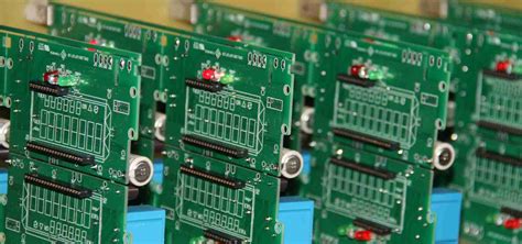
5 Design Tips for Efficient HDI PCB Manufacturing
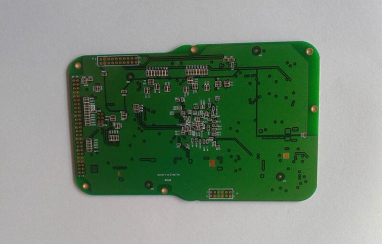
HDI PCBs are designed to maximize surface component density, provide breakout solutions for ICs with large numbers of closely spaced pins or pads, and/or carry high-frequency signals. The goal is to deliver greater functionality in a smaller package. To achieve this, you need to select a contract manufacturer (CM) with the necessary equipment and expertise to achieve the specialized requirements for HDI PCB electronics manufacturing. To optimize the manufacturing of your HDI design, you should follow a clear path or design techniques that combine your design intent with the capabilities of your CM.
Design Tips for HDI PCB Electronics Manufacturing
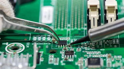
PCB layout design can be extremely complex, requiring designers to make difficult decisions about which specifications to assign the greatest importance. The process is even more complex if the design is for critical systems industries such as aerospace, medical devices, automotive or military, or for high-performance Internet of Things (IoT) or HDI. Regardless of the type of board design, designers achieve optimal results when they combine design for manufacturing (DFM) strategies with the benefits of PCB development and coordination with their CM’s capabilities.
DFM is not a one-size-fits-all approach. This is a set of rules and guidelines for specific manufacturing phases, such as Design for Assembly (DFA) and Design for Test (DFT). DFM can also focus on specific board design types, such as HDI. Let’s look at some important design tips for optimizing HDI PCB electronics manufacturing.
Tip 1: Select Via Type to Minimize Process Complexity
Via selection is a critical decision that not only determines the required equipment and manufacturing steps but also impacts processing time and additional costs. Using blind or buried microvias helps reduce layer count and material costs; however, the choice of in-pad, dog-bone, or near-pad vias can impact process complexity.
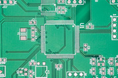
Tip 2: Select the Minimum Number of Components for HDI Applications
Component selection is always important. However, optimizing component selection is even more crucial for HDI boards. The components of an HDI design determine the trace width, location, type, and size of drilled and stacked holes. Obviously, performance is the primary consideration, but packaging, traceability, and availability should also be considered. Having to replace components or redesign the layout can lead to additional manufacturing time and material costs.
Tip 3: Space components to minimize stress and EMI
When component placement results in asymmetrical distribution of via locations, uneven stress can be applied to the board, potentially leading to warpage. This can significantly impact yield and the number of boards per panel. If components are spaced apart from densely packed high-power components, signals may introduce electromagnetic interference (EMI) into the traces, impacting signal quality. Furthermore, parasitic capacitance and/or inductance from nearby pins or pads can affect signal quality. Therefore, it is recommended to include EMI modeling during design to account for parasitic effects.
Tip 4: Route traces to minimize signal integrity issues
One of the advantages of HDI is the ability to use smaller trace widths for signal propagation. Despite reduced trace widths, traces should be designed to achieve optimal signal integrity. This includes using the shortest trace lengths, consistent path impedance, adequate ground planes, and isolation of digital, analog, and power signals.
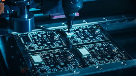
Tip 5: Select stackup to minimize material costs
In addition to selecting vias, the choice of PCB stackup also significantly impacts the manufacturing cost of HDI PCB electronics. The material type and number of layers directly impact the number of lamination and drilling cycles required. Cost should be a key factor in making these decisions.
Following the above tips for HDI PCB electronics manufacturing will help your CM make the process as efficient as possible. However, manufacturing HDI boards isn’t a one-time effort. To understand how to integrate design and manufacturing, review the following DFM for HDI case study.