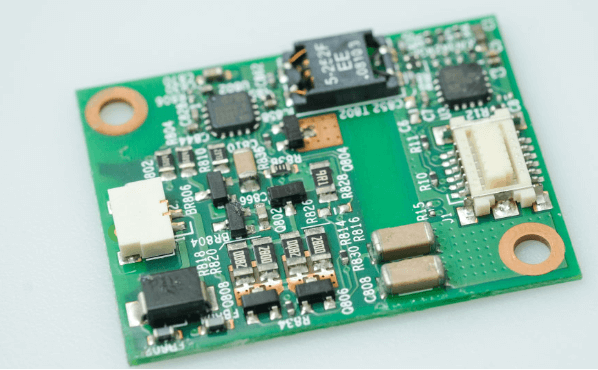
5 pcb
5 PCB design plays a vital role in modern electronic engineering. Its advantages and challenges coexist, causing designers to make comprehensive trade-offs when selecting and implementing such multi-layer circuit boards.
Provides higher circuit density
First, a significant advantage of a five-layer PCB design is its ability to provide higher circuit density. Compared with traditional single-layer or double-layer PCBs, the five-layer design allows more circuits and components to be arranged in a limited space, thereby achieving more complex functions. This is particularly important for the miniaturization and high performance requirements of modern electronic devices.
Dramatically improve signal integrity
In addition, the five-layer PCB design can significantly improve signal integrity. By increasing the number of layers, designers can better manage signal paths and reduce signal interference and crosstalk. This is especially critical for high-speed signal transmission and high-frequency applications, as any slight signal distortion may cause device performance degradation or failure. At the same time, the five-layer design also provides better power and ground distribution, helping to stabilize power supply and reduce power supply noise.
However, five-layer PCB design also faces some challenges.
The first is cost.
The manufacturing process of multi-layer PCB is complex, the material cost is high, and the production time is long. These factors result in the overall cost of five-layer PCB being significantly higher than that of single-layer or double-layer PCB. Therefore, when project budgets are limited, designers need to carefully evaluate whether a five-layer design is really necessary, or whether a similar effect can be achieved by optimizing the design.
Secondly, the complexity of five-layer PCB design also puts forward higher requirements for designers’ skills and experience.
Designers need to have in-depth circuit design knowledge and rich practical experience to effectively layout and route multi-layer PCBs. In addition, the debugging and testing of five-layer PCBs are also more complex, requiring the use of more advanced testing equipment and technology to ensure that each layer of circuits can work properly.
Nonetheless, the advantages of five-layer PCB design still make it indispensable in many high-end applications.
For example, in communications equipment, computer motherboards, and high-performance embedded systems, five-layer PCB designs can provide excellent performance and reliability. Therefore, despite the cost and complexity challenges, five-layer PCB designs remain the first choice for many engineers when pursuing high-performance and high-density circuits.
Overall, the five-layer PCB design has significant advantages in providing high circuit density and improved signal integrity, but it also faces the challenges of high cost and design complexity. By weighing these factors, designers can make the choice that best suits their project needs, resulting in the best design results.
PCB: The core and future of electronic devices
Printed circuit boards (PCBs) are the core components of modern electronic devices, and their importance cannot be ignored. As the foundation of electronic devices, PCBs not only carry various electronic components, but also realize electrical connections between components through their complex circuit design.
Whether it is smartphones, computers, home appliances or industrial control systems, PCBs play a vital role in them.
- First of all, the design and manufacturing technology of PCBs directly affect the performance and reliability of electronic devices.
High-quality PCBs can ensure the stability of signal transmission and the superiority of electrical performance, thereby improving the working efficiency and service life of the entire device. With the continuous advancement of science and technology, the design of PCBs has become more and more complex, with an increase in the number of layers and an increase in density, which have put forward higher requirements on the manufacturing process. However, advanced manufacturing technology and strict quality control enable modern PCBs to meet various high-precision and high-reliability application requirements.
- Secondly, PCBs have played a key role in promoting the miniaturization and lightweighting of electronic devices.
Traditional electronic devices are often bulky and heavy, while modern PCBs enable electronic components to be efficiently arranged in a limited space through multi-layer design and high-density wiring. This not only makes the device more portable, but also provides designers with more creative space, promoting the diversification and innovation of electronic products.
- In addition, the environmental protection characteristics of PCB are also an aspect that has attracted much attention
With the enhancement of global environmental awareness, the green design and sustainable development of electronic products have become important trends in the industry. Environmental protection technologies such as lead-free soldering and halogen-free materials are used in the modern PCB manufacturing process to reduce pollution to the environment. At the same time, the recyclability of PCB also enables waste electronic products to be effectively processed, further reducing resource waste and environmental burden.
- Finally, PCB has broad development prospects and will continue to play an important role in the advancement of electronic technology in the future.
With the rapid development of emerging technologies such as 5G communications, the Internet of Things, and artificial intelligence, the demand for high-performance and high-reliability PCBs will continue to increase. The future PCB will be more intelligent and integrated, able to adapt to more complex and diverse application scenarios, and provide a solid foundation for the innovation and development of electronic equipment.
In summary, as the core of electronic equipment, PCB is not only of great significance in terms of performance and reliability, but also plays a key role in promoting the miniaturization and environmental protection of equipment. With the continuous advancement of science and technology, PCB will continue to lead the development of electronic technology and provide a future smart life.


