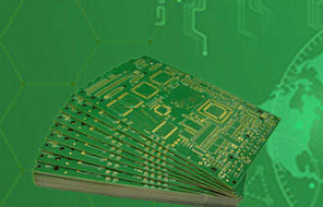
5 pcb board
Detailed explanation of the design and manufacturing process of 5 pcb board
The design and manufacturing process of 5 pcb board is a complex and delicate process involving multiple steps and technologies.
First of all, the design stage is the basis of the entire manufacturing process.
Designers need to use professional PCB design software, such as Altium Designer or Eagle, to create circuit diagrams and layouts. This stage not only needs to consider the function and performance of the circuit, but also ensure that the design meets the requirements of the manufacturing process.
Designers need to accurately plan the wiring and component layout of each layer to ensure signal integrity and electromagnetic compatibility.
Next, the design files will be converted into Gerber files, which contain detailed information on each layer.
Manufacturers will make photolithography negatives based on these files for subsequent exposure and etching processes.
During this process, any slight error may cause the function of the entire PCB board to fail, so a high degree of accuracy and professionalism is required.
In the manufacturing stage, the inner layer is first made.
The inner copper foil board will be coated with a layer of photosensitive film, and then the design pattern will be transferred to the copper foil through exposure and development processes.
Next, the excess copper is removed through the etching process, leaving only the required circuit pattern. After the inner layer is made, a lamination process is required to press the layers of copper foil and insulation materials together to form a multi-layer structure.
In a 5 PCB board, there are usually three signal layers and two power/ground layers.
Such a design helps reduce electromagnetic interference and improve signal transmission quality.
After lamination, the next step is drilling and electroplating. Drilling is to establish electrical connections between layers, usually using a high-precision CNC drilling machine.
After drilling, an electroplating process is required to plate a layer of copper on the hole wall to ensure the reliability of the electrical connection.
This process requires strict control to ensure that the copper layer thickness of the hole wall is uniform and meets the standard.
Then, the outer layer is made and the etching process is carried out, which is similar to the inner layer. After the outer layer is made, surface treatment such as hot air leveling (HASL) or chemical gold plating is required to improve welding performance and prevent oxidation.
Finally, silk screen printing and testing processes are carried out. Silk screen printing is to mark the component location and other information on the PCB board, while the testing process is to ensure that each PCB board meets the design requirements and quality standards.
In summary, the design and manufacturing process of 5 PCB boards is a highly complex and delicate process that requires multi-faceted expertise and technical support. From design to manufacturing, every step is crucial, and any slight error may affect the performance and reliability of the final product.

Therefore, only through strict process control and quality management can high-quality five-layer PCB boards be produced.
Application and Advantages Analysis of 5 PCB Boards in High-density Electronic Devices Application and Advantages Analysis of 5 PCB Boards in High-density Electronic Devices
In the design and manufacturing process of modern electronic devices, printed circuit boards (PCBs) play a vital role. Especially for high-density electronic devices, 5 PCB boards have become the first choice for many engineers and designers due to their unique structure and performance advantages.
First of all, the multi-layer structure of the 5 PCB board enables it to achieve higher circuit density in a limited space. This is especially important for high-density electronic devices that need to integrate a large number of functions and components. By increasing the number of layers, designers can arrange circuits more flexibly, reduce signal interference and electromagnetic interference, and thus improve the overall performance of the device.
In addition, the 5 PCB board also performs well in signal integrity. Due to its multi-layer structure, signals can be transmitted between different layers, thereby reducing the length and delay of the signal path.
This has significant advantages for applications with high-speed signal transmission, such as communication equipment and computer systems.
By optimizing the signal path, 5 PCB boards can effectively reduce signal loss and crosstalk, ensuring the accuracy and reliability of data transmission.
At the same time, 5 PCB boards also have good thermal management performance. In high-density electronic devices, heat management is a key issue.
Multi-layer PCB boards can improve the heat dissipation efficiency of equipment by distributing heat between different layers and reducing the heat load of a single layer.
This not only helps to extend the service life of the equipment, but also improves its working stability and reliability.
It is worth mentioning that 5 PCB boards also have significant advantages in design flexibility. The multi-layer structure allows designers to distribute power and ground lines between different layers, thereby optimizing power management and signal grounding.
This is especially important for equipment that requires high-precision power control and signal processing, such as medical instruments and avionics equipment.
Through reasonable interlayer design, 5 PCB boards can achieve higher power efficiency and lower noise levels.
Finally, 5-layer PCB boards also perform well in manufacturing costs and production efficiency. Although the manufacturing process of multi-layer PCB boards is relatively complex, its cost has been significantly reduced with the advancement of technology and the optimization of production processes.
Compared with PCBs with higher number of layers, 5-layer PCBs can provide more competitive cost advantages while maintaining high performance.
This makes its application in various high-density electronic devices more extensive and popular.
5 PCBs have become an ideal choice for high-density electronic devices due to their high circuit density, excellent signal integrity, good thermal management performance, design flexibility and cost-effectiveness. With the continuous development of electronic technology, 5-layer PCBs will show their unique advantages and broad application prospects in more fields.


