Do you know what pcb proofing is
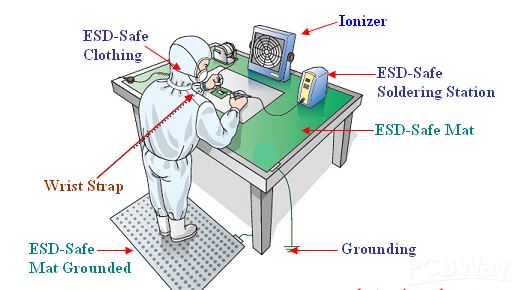
What is ESD? What are its precautions?
1.ESD literally means electrostatic discharge.
To put it simply, static electricity is a natural phenomenon that is usually generated through contact, friction, induction between electrical appliances, etc. It is characterized by long-term accumulation, high voltage (can produce several thousand or even tens of thousands of volts of static electricity), and low battery , small current and short action time. For electronic products, if the ESD design is not designed well in PCB layout design, it often causes unstable operation of electronic and electrical products.
2. Damage to electronic products
There are two types of damage and damage caused to electronic products by ESD (electrostatic discharge): sudden damage and potential damage. The so-called sudden damage refers to the device being severely damaged and losing its function. This kind of damage can usually be discovered during quality inspection during the production process, so the main cost to the factory is rework and repair costs. Potential damage refers to parts of the device being damaged, but the function has not been lost, and cannot be found during the inspection of the circuit board production process. However, during use, the product will become unstable and sometimes good or bad, thus posing a negative impact on product quality. Greater harm.
Among these two types of damage, latent failure accounts for 90%, and sudden failure accounts for only 10%. In other words, 90% of electrostatic damage cannot be detected and will only be discovered when it is used in the user’s hands. Problems such as frequent freezes, automatic shutdowns, poor voice quality, loud noises, intermittent signal quality, and wrong keystrokes on mobile phones are mostly related to electrostatic damage. Because of this, electrostatic discharge is considered the biggest potential killer of electronic product quality, and electrostatic protection has also become an important part of electronic product quality control. The difference in stability between domestic and foreign brands of mobile phones during use basically reflects their differences in electrostatic protection and anti-static design of the products.
If electronic products such as PCB boards have no problems in R&D technology, once a failure occurs, it is mostly related to ESD static electricity. As we all know, ESD static electricity is everywhere. For some tiny electronic components, as long as they are broken down by static electricity, the entire production line will also face collapse.

GET PCB MANUFACTURING AND ASSEMBLY QUOTE NOW!
what impact does static electricity have on electronic components?
1. The basic physical properties of static electricity are the following three:
attraction or repulsion, potential difference with the earth, and discharge current.
2. The impact of these three characteristics on electronic components:
(1) Electrostatic adsorption of dust reduces the insulation resistance of components, thereby shortening component life.
(2) Heat generated by electrostatic discharge or current may cause potential damage to components.
(3) The electromagnetic field generated by electrostatic discharge has a large amplitude and extremely wide spectrum, causing interference or even damage to electronic devices.
(4) Electrostatic discharge damage causes components to be damaged and unable to work.
It can be seen that the harm of ESD static electricity is immeasurable, and enterprises should do comprehensive protection work to prevent losses caused by ESD static electricity hazards.
GET PCB AND ASSEMBLY SERVICE QUOTE NOW!
What impact does static electricity have on electronic components?
1. The basic physical properties of static electricity are the following three: attraction or repulsion, potential difference with the earth, and discharge current.
2. The impact of these three characteristics on electronic components:
(1) Electrostatic adsorption of dust reduces the insulation resistance of components, thereby shortening component life.
(2) Heat generated by electrostatic discharge or current may cause potential damage to components.
(3) The electromagnetic field generated by electrostatic discharge has a large amplitude and extremely wide spectrum, causing interference or even damage to electronic devices.
(4) Electrostatic discharge damage causes components to be damaged and unable to work.
It can be seen that the harm of ESD static electricity is immeasurable, and enterprises should do comprehensive protection work to prevent losses caused by ESD static electricity hazards.
What should we pay attention to
1. Use multi-layer PCB whenever possible
Compared with a double-sided PCB, the ground plane and power plane, as well as the tightly arranged signal line-ground line spacing, can reduce the common mode impedance and inductive coupling to 1/10 to 1/100 of the double-sided PCB. Try to place each signal layer as close to a power or ground layer as possible. For high-density PCBs that have components on both the top and bottom surfaces, very short connecting traces, and lots of ground fill, consider using inner-layer traces.
2. For double-sided PCBs, use a tightly interwoven power and ground grid.
Place the power wires next to the ground wires, with as many connections as possible between vertical and horizontal wires or padded areas. The grid size on one side should be less than or equal to 60mm. If possible, the grid size should be less than 13mm.
3. Make sure every circuit is as compact as possible.
4. Keep all connectors aside as much as possible.
5. The same “isolation zone” should be set up between the chassis ground and circuit ground on each layer; if possible, keep the separation distance at 0.64mm.
6. When assembling PCB, do not apply any solder on the top or bottom pads.
Use screws with inline washers to achieve tight contact of the PCB with the metal chassis/shield or bracket on the ground plane.
7. If possible, route the power cord from the center of the card and away from areas prone to direct ESD effects.
8. On all PCB layers below the connectors leading out of the chassis (easily hit by ESD directly), place wide chassis grounds or polygon fill grounds, and connect them with vias at intervals of approximately 13mm. Together.
9. Place mounting holes on the edge of the card and connect the top and bottom solder mask-free pads around the mounting holes to the chassis ground.
10. On the top and bottom layers of the card close to the mounting holes, connect the chassis ground and circuit ground together with a 1.27mm wide line along the chassis ground wire every 100mm. Adjacent to these connection points, place pads or mounting holes for mounting between chassis ground and circuit ground. These ground connections can be slit with a razor blade to keep them open, or jumpered with ferrite beads/high frequency capacitors.
11. If the circuit board will not be placed in a metal chassis or shielding device, do not apply solder resist to the top and bottom chassis ground wires of the circuit board so that they can serve as discharge electrodes for the ESD arc.
layout design
12. Set up a ring ground around the circuit in the following manner:
(1) Except for the edge connector and the chassis ground, place a circular ground path around the entire periphery.
(2) Ensure that the annular width of all layers is greater than 2.5mm.
(3) Connect the annular ground with via holes every 13mm.
(4) Connect the ring ground to the common ground of the multi-layer circuit.
(5) For double panels installed in metal chassis or shielding devices, the ring ground should be connected to the circuit common ground. For unshielded double-sided circuits, the ring ground should be connected to the chassis ground. The ring ground should not be coated with solder resist so that the ring ground can act as an ESD discharge rod. Place at least one somewhere on the ring ground (all layers). 0.5mm wide gap to avoid forming a large loop. The distance between the signal wiring and the ring ground should not be less than 0.5mm.
13. In areas that can be directly hit by ESD, a ground wire must be laid near each signal line.
14. The I/O circuit should be as close as possible to the corresponding connector.
15. Circuits that are susceptible to ESD should be placed near the center of the circuit so that other circuits can provide a certain shielding effect for them.
16. A transient protector is usually placed at the receiving end. Use a short and thick wire (length less than 5 times the width, preferably less than 3 times the width) to connect to the chassis ground. The signal wires and ground wires coming out of the connector should be connected directly to the transient protector before being connected to other parts of the circuit.
17. Usually, series resistors and magnetic beads are placed at the receiving end. For cable drivers that are easily hit by ESD, you can also consider placing series resistors or magnetic beads at the driving end.
The layout design should place filter capacitors at the connector or within 25mm from the receiving circuit.
(1) Use a short and thick wire to connect to the chassis ground or receiving circuit ground (the length is less than 5 times the width, preferably less than 3 times the width).
(2) The signal line and ground line are connected to the capacitor first and then to the receiving circuit.
18. When designing the layout, ensure that the signal lines are as short as possible.
19. When the length of the signal line is greater than 300mm, a ground wire must be laid in parallel.
20. Ensure that the loop area between the signal line and the corresponding loop is as small as possible. For long signal lines, the positions of the signal line and the ground wire should be exchanged every few centimeters to reduce the loop area.
21. Drive signals from a central location in the network into multiple receive circuits.
22. Where possible, fill in unused areas with land and connect all layers of fill at 60mm intervals.
23. Ensure that the loop area between power and ground is as small as possible, and place a high-frequency capacitor close to each power pin of the integrated circuit chip.
24. Place a high-frequency bypass capacitor within 80mm of each connector.
25. Reset lines, interrupt signal lines or edge trigger signal lines cannot be arranged close to the edge of the PCB.
26. Ensure that the two opposite end points of any large ground filling area (approximately greater than 25mm&mes;6mm) are connected to the ground.
27. When the length of the opening on the power or ground plane exceeds 8mm, use a narrow wire to connect both sides of the opening.
28. The layout design connects the mounting holes to the circuit common ground, or isolates them.
(1) When the metal bracket must be used with a metal shielding device or chassis, a zero-ohm resistor must be used to connect it.
(2) Determine the size of the mounting holes to achieve reliable installation of metal or plastic brackets. Use large pads on the top and bottom layers of the mounting holes. Solder resist cannot be used on the bottom pads, and ensure that the bottom pads do not use wave soldering processes. welding.
29. Protected signal lines and unprotected signal lines cannot be arranged in parallel.
30. Layout design should pay special attention to the wiring of reset, interrupt and control signal lines.
(1) High-frequency filtering must be used.
(2) Keep away from input and output circuits.
(3) Stay away from the edge of the circuit board.
31. The PCB should be inserted into the chassis and should not be installed in openings or internal seams.
32. Pay attention to the wiring under the magnetic beads, between the pads and the signal lines that may come into contact with the magnetic beads. Some magnetic beads conduct electricity quite well and may create unexpected conductive paths.
33. If a chassis or motherboard is to contain several circuit boards, the circuit board that is most sensitive to static electricity should be placed in the center. The above is how to prevent ESD in PCB layout. I hope it can help you.