How to select circuit materials from the perspective of thermal management in 5G technology applications
With the rise of the Internet of Things and the increasing abundance of mobile Internet content, people have put forward higher requirements for the transmission rate and service quality of mobile communication networks. The fifth generation (5G) wireless mobile communication technology emerged and developed rapidly. At the same time, 5G will also penetrate into various other industry fields and be deeply integrated with industrial facilities, medical instruments, Internet of Vehicles, etc., effectively meeting the diverse business needs of industry, medical care, transportation and other industries, and realizing the true “Internet of Everything” .
High-frequency millimeter waves have significant advantages in 5G communications, such as sufficient bandwidth, miniaturized antennas and equipment, and high antenna gain. The four high-frequency bands planned by the U.S. Federal Communications Commission for 5G include 3 licensed bands and 1 unlicensed band. However, finding printed circuit board (PCB) materials with excellent performance and affordable prices in these bands is a huge challenge. Therefore, it is crucial to correctly understand the key parameters and characteristics of PCB materials and select PCB materials suitable for application within the 5G technology application frequency band.

Next, we will discuss how to select PCB materials suitable for applications within the 5G technology application frequency band from the perspective of thermal managem
GET PCB MANUFACTURING AND ASSEMBLY QUOTE NOW!
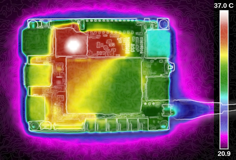
Thermal management
When high-frequency/microwave RF signals are fed into a PCB circuit, losses caused by the circuit itself and circuit materials will inevitably generate a certain amount of heat. In the application of 5G equipment, not only the frequency of use is increasing, but the equipment also tends to be miniaturized, which is bound to generate more heat. Handling circuit thermal management and understanding the thermal characteristics of PCBs can help avoid circuit performance degradation and reduced reliability caused by high temperatures.
1. Thermal model
In a microstrip line circuit, the top signal plane is the circuit heat source, the bottom ground plane is the low-temperature area or heat dissipation plane, and the two planes are filled with dielectric material. In the thermal model, heat will be transferred from the signal plane through the material to the low-temperature region of the ground plane for heat dissipation. Although the heat generation process of actual microstrip line circuits is complex, for simple thermal models, such an assumption is acceptable. k in the heat flow equation is the heat conduction system of the material, A is the area of the heat source, L is the thickness of the material, and (TH-TL) is the temperature difference between the upper and lower sides. Heat flow equations and thermal models explain that choosing circuit materials with high thermal conductivity and thin thickness can achieve better heat dissipation and heat management.
2. Thermal management
Designers usually evaluate temperature rise from the perspective of circuit efficiency and loss, but the PCB medium, as the nearest thermal conductor to the heat source, has a greater impact on temperature rise. As shown in Figure 6, we can find through simulation that among commonly used plates, the method of reducing the temperature rise by reducing the Df value of the plate is not as effective as using a higher thermal conductivity method. Although the dielectric loss in different materials will ultimately affect the insertion loss of the circuit, resulting in different amounts of heat, the thermal conductivity of the material is more obvious for temperature changes. For the same thermal conductivity value, such as 0.4W/m/K, the temperature rise caused by the dielectric loss Df from 0.001 to 0.004 is only about 0.22°C/W. However, even for materials with the same Df of 0.001, a change in thermal conductivity from 0.2W/m/K to 1.5W/m/K can cause a temperature drop of 0.82°C/W. If the input power of the circuit is 50W, then the temperature can be reduced by about 40°C.
In addition to the thermal conductivity of the material, some other parameters of the material also have an impact on heat management. In order to better understand the influencing factors related to the thermal performance of PCB circuits, the temperature change results of circuits based on different materials, different material thicknesses, loss factors, thermal conductivity, copper foil roughness and insertion loss are shown. This table provides a reference for comparing the thermal effects of different circuit materials. Comparing circuit No. 1 and circuit No. 2, the difference between the two is the thickness of the circuit, so changes in the thickness of the PCB material will lead to differences in temperature rise. The thinner the thickness, the shorter the heat dissipation path, and the lower the temperature rise under the same conditions; comparing circuits No. 2 and No. 3, the difference between the two is mainly the difference in insertion loss caused by different copper foil roughness. The smaller the surface roughness of the copper foil, the lower the insertion loss and the smaller the temperature rise; the material of circuit 4 is FR-4, which is basically not used in the microwave/millimeter wave band. As an example, it can be seen that FR-4 has shortcomings in multiple aspects, such as high dielectric loss, conductor loss and lower thermal conductivity, thus having the highest insertion loss under the same circuit, resulting in a significant increase in temperature rise. Circuit 5 is based on Rogers RT/duroid 6035HTC PTFE ceramic material, which has a thermal conductivity of up to 1.44W/m/K and has the best thermal conductivity characteristics while having a very low loss factor and the lowest insertion loss at the same input power It has the lowest temperature rise and is very suitable for high-power microwave applications.
Therefore, for heat management of circuits, relatively thin circuit materials should be selected. At the same time, selecting material properties such as high thermal conductivity, smooth copper foil surface, and low loss factor will help reduce the heating of circuits in the microwave and millimeter wave frequency bands.
3.Multilayer board design
5G technology not only requires smaller base station equipment, but also requires smaller antenna sizes. At the same time, active antenna systems that combine active circuits with antennas will serve as an important part of the upcoming 5G network. Miniaturized designs and active antenna systems require circuits to use more multi-layer board designs.
4.Z-axis thermal expansion coefficient
The thermoplastic material commonly used for high-frequency PCB boards is polytetrafluoroethylene, which can be reinforced with various forms of fillers such as fiberglass or ceramic materials. Compared with thermoset materials, PTFE thermoplastic materials usually have better electrical properties and smaller electrical losses, but the Z-axis thermal expansion coefficient of PTFE materials is much higher than that of copper. When making multi-layer boards, when the circuit board passes through high temperatures, different expansions occur due to different thermal expansion coefficients between the material and copper, causing the reliability of PTH vias to fail.
The importance of choosing materials with low thermal expansion coefficients for the reliability of vias in high-frequency multilayer board applications is self-evident. Rogers Company’s research has found that adding some special ceramic fillers to PTFE thermoplastic materials can improve the thermal expansion coefficient of the material. Combining the low temperature characteristics and electrical characteristics of the PTFE material itself, this material is very suitable for the application of high-frequency millimeter wave multilayer boards. For example, Rogers’ RO3000 series circuit board materials have a Z-axis thermal expansion coefficient as low as 24ppm/°C. High-reliability vias can be completed using only a simple plasma treatment process; and it has extremely low dielectric loss. , very suitable for circuit design of high-frequency multilayer boards.
5. Impedance matching
The design and processing control of vias in high-frequency microwave/millimetre-wave multilayer circuit boards are also aspects that need attention. In the design and processing of via holes, the size of the via hole, the thickness of the copper in the hole, the size of the pad on the outer surface of the hole, and the distance between the hole and the ground plane will all affect the parasitic capacitance and parasitic inductance of the via hole. This affects the distribution parameters of the vias and leads to mismatch of the overall circuit. This situation is more obvious in the microwave/millimeter wave frequency band. Laminate 8mil RO4450F hydrocarbon ceramic prepreg on both sides of the 7.3mil Rogers RO4350B Lopro copper-clad board to produce 4 layers each containing through-hole microstrip circuits. Through experiments, we found that comparing through-hole circuits, which have the same through-hole length and copper thickness, but smaller aperture and smaller hole pad, have smaller parasitic capacitance, better broadband characteristics and return loss, Figure 8 shows the measured data of improving circuit return loss and RF bandwidth by reducing the impedance step change caused by reducing the through hole aperture and hole pad.
GET PCB AND ASSEMBLY SERVICE QUOTE NOW!
Generally speaking
the continuous development of 5G technology and the demand for microwave frequency bands have put forward higher requirements for the performance of PCB materials. Choosing the appropriate board thickness according to the frequency, selecting PCB materials with small loss factors, understanding the impact of the surface roughness of the copper foil of the PCB material and selecting different copper foils, and appropriate surface treatment processes will help reduce the insertion loss of the circuit. PCB materials with high thermal conductivity are conducive to heat management of smaller size and higher integrated circuits in 5G applications to achieve the best heat dissipation solution. At the same time, the appropriate PCB material type, thermal expansion coefficient of the material, via processing and reliability performance will ultimately determine the material selection.