pcb assembly guidelines
What is PCB assembly
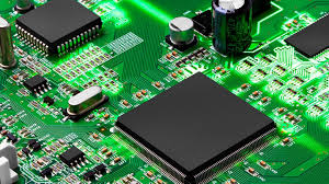
The circuit board before assembling the electronic components is called PCB. Once the electronic components are soldered, the board is called Printed Circuit Assembly (PCA) or Printed Circuit Board Assembly (PCBA) or PCB Assembly. Different manual and automatic PCB assembly tools are used in this process.
It is important to note that the assembly of the circuit board is different from the PCB manufacturing process. There are several processes involved in manufacturing printed circuit boards, including PCB designing and creating PCB prototypes. Once the PCB is ready, active and passive electronic components need to be soldered to it before it can be used in any electronic device or gadget. This assembly of electronic components depends on the type of printed circuit board, the type of electronic components, and the purpose of the circuit board.
GET PCB MANUFACTURING AND ASSEMBLY QUOTE NOW!
Things Needed for PCB Assembly
Post PCB Assembly Tools Electronic Components and Consumables Needed for PCB Assembly -PCB:
Basic Electronic Components
Soldering Materials include Solder Wire, Solder Paste, Solder Bar, Solder Ball BGA, Solder Preform (depending on the type of soldering to be done)
Flux
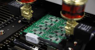
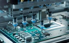
Soldering Equipment includes Soldering Station, Wave Soldering Machine, SMT Equipment, Inspection and Testing Equipment, etc.
Once all the above equipment, electronic components and all raw materials are arranged, the PCB assembly process can begin.
PCB Assembly with Through-Hole Electronic Components
Electronic components with leads inserted through small holes in the PCB for soldering are called through-hole electronic components.
The assembly or soldering process of these components includes wave soldering and wave soldering hand soldering.
Wave Soldering – During the PCB assembly process, solder is placed in a high temperature tank in the form of a solder bar. This solder is left in a molten form in a molten pool and forms a wave shape at a very high temperature
The range of temperature depends on the type of solder. Traditional Tin/Lead (Sn/Pb) solder has a lower melting point than Lead-Free (Pb-Free) soldering. With the help of conveyor belt, PCB with all through hole electronic components are desoldered.
GET PCB AND ASSEMBLY SERVICE QUOTE NOW!
The whole wave soldering PCB assembly process includes the following steps:
Inserting electronic components
Application of flux
Preheating
Wave soldering
Cleaning
Testing
The processing after wave soldering is completed is cleaning and testing. If there are any faults or defects in solder joints such as pinholes or blown holes, wave soldering defects are found and sent for rework, generally manual rework.
Manual soldering is carried out in production units with small workloads or in rework/repair work. Good quality soldering stations or soldering irons, solder wires and flux are used in this process.

PCB circuit board assembly production guide
I. PCB writing technical specifications
Preparing project specifications is an important part of PCB design. It may include technical requirements, block diagrams, deliverables, assumptions, preliminary bill of materials (BOM) and BOM costs, tools and techniques developed for project development.
The more adequate the preliminary preparation, the fewer problems you may encounter in the hardware design process. In hardware design, the author has encountered more than once that he had to change the solution due to problems in hardware design, or even that he had completed the sample but found that some functions could not be completed. These problems can be avoided in the demand design stage.
2. PCB Schematic Design
The process of PCB board design always starts with a schematic. The schematic or circuit diagram conveys the electrical connection between different electrical components such as integrated circuits (ICs) and discrete components.
Generally, professional CAD software such as Altium Designer, PADS, Cadence Allegro and other software are used to define the module and design the connection between different components. The schematic determines the working principle of the PCB. In the schematic design stage, we need to complete the electrical connection of the hardware and determine the package size of the device.
3. Printed Circuit Board Layout
Once the schematic is imported into the PCB layout, the components are manually placed on the circuit board and routed. Because the number of required layers and the size of the components are taken into account, these sizes may be limited by the size of the shell.
In the PCB layout design, we analyze the signal integrity and evaluate the electrical limitations to ensure the safety of the board-level architecture. For complex layouts, it is also necessary to use various simulation tools to ensure the integrity of the signal, the reliability of the design, etc. When designing the circuit, it is necessary to take some precautions to ensure that its EMC performance requirements can be met.
Once the circuit design and construction are completed, it will be more difficult and expensive to try to fix the EMC performance. Many aspects can be addressed during the circuit design and PCB layout stages to ensure that EMC performance is optimized: PCB circuit design—PCB circuit partitioning—PCB grounding—PCB routing—EMC filters—I/O filtering and shielding. By taking these precautions, the EMC performance of the PCB layout can be greatly improved.
Circuit board design is a link in hardware development that requires a lot of effort. Many simulation tools are needed during the design process to perform reliability design to minimize PCB design revisions, reduce development costs, and shorten the R&D cycle.
4. Printed Circuit Board Manufacturing and Testing
Once our PCB design layout is approved for production, it needs to be exported to a format supported by the manufacturer. Prepare a bill of materials (BOM) and Gerber files that describe the design requirements for each image of the circuit board. The manufacturer uses this document as a reference for circuit board manufacturing and PCB assembly.
For some projects, it is also necessary to create a 3D model of the PCB to ensure that it fits the enclosure. Testing is essential for both the PCB layout design service and the manufacturing stage. On high-speed PCBs and RF boards, it is also necessary to provide the manufacturer with the data and software required to perform resistance and impedance testing. After the sample is manufactured, it needs to be tested internally.
5. PCB mass production
After prototype verification, prepare documents for mass production and provide assistance to the production department throughout the manufacturing process. Special software, hardware and test procedures need to be provided to the production department. Write detailed test operation instructions and provide test indicators to ensure that the products produced and put into storage are in compliance with standards.