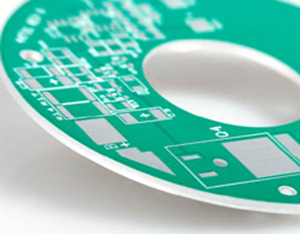
How to made ceramic pcb prototype ?
To make a ceramic PCB prototype, you can follow these steps:
1. Design the PCB: Use a PCB design software (e.g., Altium, Eagle) to create the layout and circuit design
of your PCB. Ensure that you consider the specific requirements and constraints of ceramic PCBs, such
as the material properties and manufacturing processes.
2. Choose the ceramic material: Select the appropriate ceramic material for your PCB prototype. Common
ceramic materials used for PCBs include alumina (Al2O3) and aluminum nitride (AlN). Consider the electrical,
thermal, and mechanical properties of the material based on your application requirements.
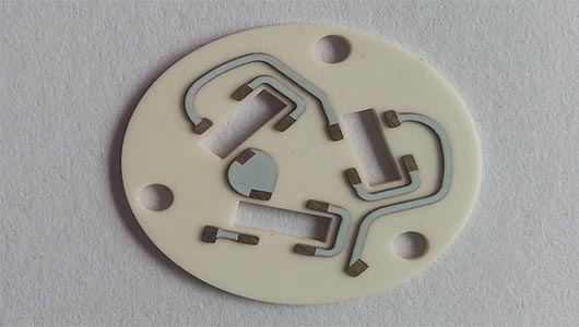
3. Prepare the ceramic substrate: Start with a blank ceramic substrate and prepare
it for the PCB manufacturing process. Clean the surface thoroughly to remove any
contaminants or impurities.
4. Apply the conductive traces: Use a screen printing or thick film deposition method
to apply the conductive traces onto the ceramic substrate. This involves using a stencil
or mask to deposit a conductive paste or ink onto the substrate. Ensure that the traces
are accurately placed and have the desired width and thickness.
5. Cure the conductive traces: After applying the conductive traces, the substrate needs
to be cured. This can be done by placing it in a high-temperature furnace or oven to allow
the conductive material to solidify and adhere to the ceramic substrate.
6. Apply the solder mask: Apply a solder mask over the cured conductive traces
to protect them from oxidation and to provide insulation. The solder mask can be
applied using a screen printing or spray coating method.
7. Cure the solder mask: Similar to the conductive traces, the solder mask needs
to be cured. Place the substrate in a furnace or oven at the appropriate temperature
and duration to ensure proper curing.
8. Drill holes and vias: Use a laser or mechanical drilling method to create holes and
vias in the ceramic substrate. These holes will be used for component mounting and interconnection.
9. Apply surface finish: Apply a surface finish to protect the conductive traces
and provide a solderable surface. Common surface finishes for ceramic PCBs
include gold plating and tin plating.
10. Test and inspect the prototype: Once the manufacturing process is complete,
test and inspect the ceramic PCB prototype for functionality, electrical continuity,
and quality. Make any necessary adjustments or improvements before moving
forward with mass production.

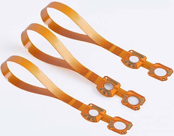
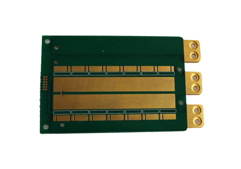
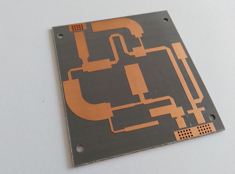
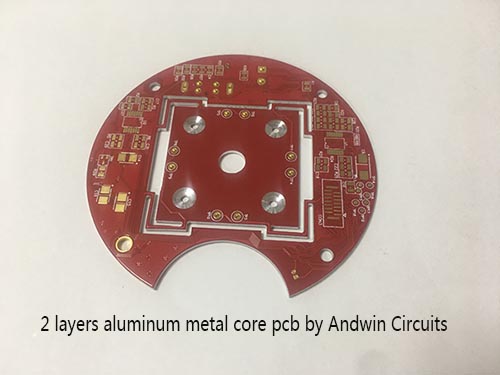
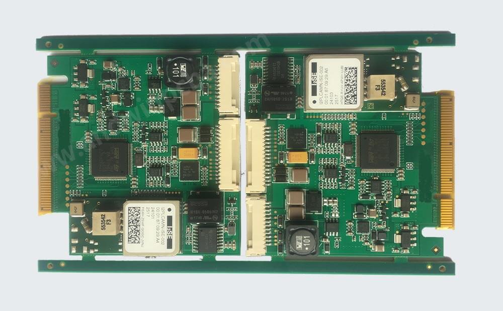
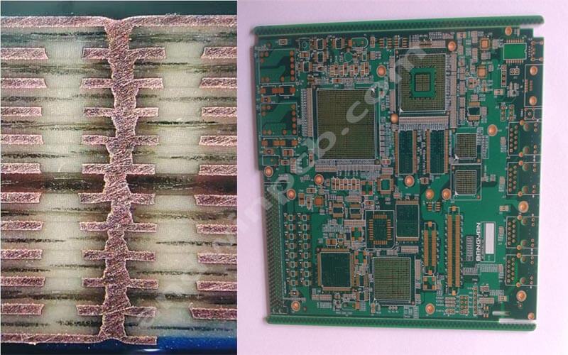
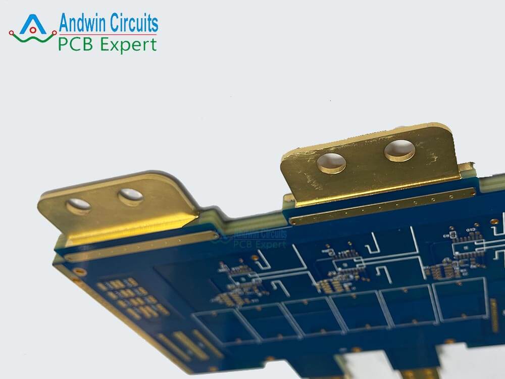
Other PCB products, you may interesting