2 layer pcb vs 4 layer pcb
What are the layers of a circuit board used for?
The most important layer in a PCB circuit board is the copper trace layer, which is how the PCB got its name. While a 2-layer PCB has two trace layers, a 4-layer PCB has four trace layers.
These trace layers are used to connect to other electronic components in a device. In between these layers are insulating layers or cores, which are added between the trace layers to give it structure.
In a 4-layer PCB, there is also a solder mask layer, which is applied on top of the signal layer.
This prevents the copper traces from interfering with other metal components on the PCB. They also have a silk screen layer that is used to add numbers to the different components to make them easier to understand.
With PCB printed circuit boards, there are endless possibilities for the number of layers you can design. Some supercomputers have circuit board structures with nearly a hundred layers, however, the most common boards are usually two or four layers. 2-layer PCBs Compared to 4-layer PCBs, 2-layer PCBs are easier to use due to their simple design. While not as simple as 1-layer PCBs, they are as simple as possible without sacrificing the ability to have double-sided inputs. The reduced complexity leads to an equally reduced price tag, but it means fewer possibilities compared to 4-layer PCBs.
However, as a professional, there is no propagation delay for the signal.
4-layer PCB is the simplest type of multi-layer circuit board, which greatly improves the electromagnetic compatibility of the circuit board compared to 2-layer PCB.
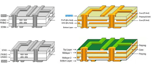
4-layer PCB has a larger surface area than 2-layer PCB, increasing the possibility. Among all multi-layer circuit board types, the most common is 4-layer PCB. The stacking of 4-layer PCB is very solid, it includes top layer, inner layer 1, inner layer 2 and bottom layer for routing electrical signals.
Both inner layers are located between the top layer and the bottom layer. Therefore, 4-layer PCB means 2 signal layers + one positive voltage layer (VCC layer) + one ground layer (GND layer) or 3 signal layers + GND layer.
In 4-layer PCB design, more surface area can be used for routing. Therefore, this design structure provides excellent routing for low-speed and high-speed signals. Therefore, they are very suitable for more complex devices.
Two-layer PCB, PCB two-layer board and four-layer board difference?
In the design and manufacturing process of PCB, different number of layers will affect the performance, wiring and cost of the circuit. At present, two-layer PCB and four-layer PCB are the most commonly used PCB types. So, what is the difference between two-layer board and four-layer board?
1.Design
Two-layer PCB has a simple design. They have only two layers of copper foil: top layer and bottom layer. Wiring is only done on the top and bottom layers, and crossing is not allowed during wiring, making wiring more difficult. Therefore, they are usually used for simple applications, and the design does not contain complex high-speed signal lines or power circuits.
Four-layer PCB consists of four layers of copper foil: top layer, ground layer, power layer and bottom layer. Among them, the ground layer and power layer are internal layers, and wiring can be done in the X and Y directions. This structure can reduce the interference of signal jumpers and EMI on the PCB, so they are often used in high-end applications that require the layout of complex circuits or high-density components.
2.Manufacturing
Two-layer PCB is simple to manufacture and low cost, and can use conventional noble metallization (HASL), lead-free noble metallization (ENIG) or organic molybdenum copper (OSP) and other surface treatment methods.
The manufacturing of four-layer PCB is more complicated, requiring the use of micro-circuit board manufacturing technology (MLL), adding power layer and ground layer connection circuit in the inner layer, and using blind hole drilling and other processing technologies to achieve wiring on the outside. Therefore, the manufacture of four-layer boards requires higher technology and cost.
3.Cost
It is cheaper to produce two-layer PCB than four-layer PCB. Often used in large industrial projects or consumer electronics. However, for high-frequency communication applications or situations that require noise resistance, it is recommended to use a four-layer PCB.
4.Performance
Two-layer PCB wiring is limited and is not suitable for high-speed and high-frequency applications. At the same time, two-layer boards are more susceptible to EMI and noise interference, and layout is also more difficult.
Because the inner layer connection process of the four-layer PCB does not affect its front side, all devices can be routed on the front side, and internal power layers and ground layers can be added to enhance EMI suppression capabilities. It can be applied to complex circuits, high-speed signals, and electronic devices equipped with complex components.
In short, the difference between two-layer PCB and four-layer PCB is in design, manufacturing, cost, and performance. It is particularly important to choose the right PCB type according to the functions and details required for the specific application. Therefore, you should know more about the differences between the types to find the most suitable solution.