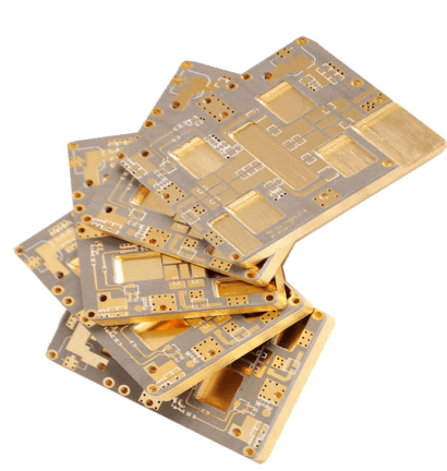
4 layer metal core pcb
what is metal core pcb
MCPCB metal core printed circuit board is the PCB aluminum substrate we see in the field of LED lighting. Metal core PCB is also called insulated metal substrate, insulated metal PCB and metal clad PCB. In this article, we will use the abbreviation MCPCB to avoid ambiguity. MCPCB consists of an insulation layer, a metal plate and a metal copper foil. The basic structure of MCPCB includes the following: solder mask, circuit layer, copper layer 1 ounce-6 ounces (most commonly 1 ounce to 2 ounces), dielectric layer and metal core layer.
Compared to traditional FR4 boards, it is based on metal materials for the heat sink segment of the board. Metal core boards transfer heat 8 to 9 times faster than FR4 boards.
These metal core laminates keep heat-generating components cooler by dissipating heat at a faster rate. The dielectric material should be kept as thin as possible so that it forms the shortest path from the heat source to the metal backplane.
This helps in faster heat dissipation. The thickness of the dielectric material will typically range from 0.076mm to 0.152mm.
Metal core PCBs are used where a lot of heat is generated in the circuit, so the heat needs to be dissipated quickly to avoid damaging the components.
During the operation of the board, heat is generated due to certain electronic components.
The purpose of the metal is to transfer heat from critical board components to secondary areas such as the backing or metal core of the metal heat sink. Therefore, these PCBs are easy to thermally manage.
Multilayer PCB is the product of the development of electronic information technology towards high speed, multi-function, large capacity, small size, thinness and light weight. For the production of PCB boards, the more layers there are, the more production procedures there are, and the failure rate will increase accordingly, and the corresponding cost will be higher, so generally multilayer boards are used in advanced circuits.
The four layers in the four-layer PCB board are divided into:
- signal layer (top layer)
- signal layer (bottom layer)
- power layer (middle layer)
- ground layer (middle layer).
Usually in the circuit board, the top layer is generally used to place components, so the top layer is also called the component surface; the bottom layer is generally used for welding, so the bottom layer is also called the welding surface. But for SMD components, both the top and bottom layers can be used to place components.
The four layers in the four-layer PCB board are divided into: signal layer (top layer), signal layer (bottom layer), power layer (middle layer) and ground layer (middle layer).
Usually in the circuit board, the top layer is generally used to place components, so the top layer is also called the component surface; the bottom layer is generally used for welding, so the bottom layer is also called the welding surface. But for SMD components, both the top and bottom layers can be used to place components.
In our lives, electronic products are everywhere, such as smartphones for convenient communication, laptops used at work, wearable watches, etc. No matter what kind of electronic product, different types of PCB boards are included in the manufacturing process. Then let’s follow this article to learn about the advantages of the 4-layer PCB board structure.
- Hierarchical design
The traditional double-layer board has defects such as crowded wiring and cross interference. This product adds an inner conductive layer and an insulating dielectric layer during the design process to make the overall design more hierarchical, while also increasing the flexibility and efficiency of circuit board wiring, improving the wiring density of the circuit board, and making the signal transmission path more convenient, thereby improving the overall performance. - Complete signal transmission
How to measure the performance of the circuit board, the answer is to see whether the signal transmission is complete. The overall structure of this product has been optimized, and the inner layer setting is more reasonable, so that the signal line can be directly and efficiently connected, preventing the signal from being attenuated or distorted during transmission, thereby ensuring reliable signal transmission. - Power management efficiency
Since a dedicated power supply and grounding line is set in the inner conductive layer, the power distribution can be effectively managed, which can avoid electromagnetic interference and reduce voltage fluctuations. At the same time, it can also improve the efficiency of power management, effectively reduce system energy consumption, and truly achieve energy conservation and environmental protection. - Long service life
During the operation of electronic equipment, a common problem is heat dissipation, which can directly affect the stability of the system. The advantages of the 4-layer PCB board structure are mainly reasonable layer layout, selection of high-quality thermal conductive materials, and effective improvement of the heat dissipation performance of the circuit board. In particular, the conductive layer can serve as a heat dissipation channel, which can quickly transfer heat to the external heat dissipation device, maintain the appropriate temperature of the system, and extend the service life. - Electromagnetic compatibility
By adding shielding layers and filters, the impact of electromagnetic interference on the system can be reduced and electromagnetic compatibility can be improved.
The advantages of the 4-layer PCB board structure also include convenient assembly and maintenance, because the layout between components is clear and reasonable, which can reduce the difficulty and complexity of assembly. If problems occur during use, the staff can have a larger operating space to repair, and timely inspect and replace the damaged devices. Although the price of this product is relatively expensive, it can save the cost of repairing and replacing equipment in the long run, and it is worth choosing.