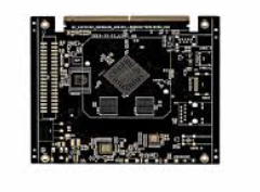
6 layer pcb motherboard
Detailed explanation of the design and manufacturing process of 6 layer PCB motherboard
The design and manufacturing process of 6 ayer PCB motherboard is a complex and sophisticated process involving multiple steps and technical details.
First of all, the design stage is the basis of the entire manufacturing process.
Designers need to use professional electronic design automation (EDA) software to create circuit diagrams and layout diagrams. At this stage, designers must consider factors such as signal integrity, power integrity and thermal management to ensure the performance and reliability of the final product. Through reasonable stacking structure design, electromagnetic interference (EMI) and crosstalk can be effectively reduced, thereby improving the stability of the circuit.
Next, the design files will be converted into manufacturing files, which include Gerber files, drilling files, and assembly drawings.

These files will be sent to PCB manufacturers as the basis for production. In the manufacturing stage, the first thing to do is material selection.
Usually, 6 layer PCB motherboards use FR4 as the substrate, which has good electrical properties and mechanical strength. Then, the manufacturer will laminate according to the design files, stack the layers of copper foil and insulation materials together, and cure them through high temperature and high pressure.
After the lamination is completed, drilling and electroplating will follow.
Drilling is to establish electrical connections between layers, and is usually done using a high-precision CNC drilling machine. After drilling is completed, an electroplating process is performed to plate a layer of copper on the hole wall to ensure the reliability of the electrical connection. Subsequently, a pattern transfer is performed, the circuit pattern is transferred to the copper foil through a photolithography process, and the excess copper is removed through an etching process to form the desired circuit pattern.
After the pattern transfer and etching are completed, surface treatment is performed.
Common surface treatment methods include hot air leveling (HASL), chemical nickel-gold plating (ENIG), and organic coating (OSP). The purpose of surface treatment is to protect the copper surface, prevent oxidation, and improve welding performance. Next is the filling and covering of pads and vias to ensure welding reliability and electrical performance.
Finally, electrical testing and quality inspection are performed. Electrical testing includes open and short circuit tests to ensure the integrity and functionality of the circuit. Quality inspection includes appearance inspection and dimensional measurement to ensure that the product meets design requirements and industry standards. Through these rigorous tests and inspections, the high quality and reliability of the 6 layer PCB motherboard can be ensured.
In summary, the design and manufacturing process of 6 layer PCB motherboard is a multi-step and precise process, and each link is crucial. Through reasonable design, precise manufacturing and rigorous testing, high-performance and high-reliability 6-layer PCB motherboards can be produced to meet the needs of various complex electronic devices.