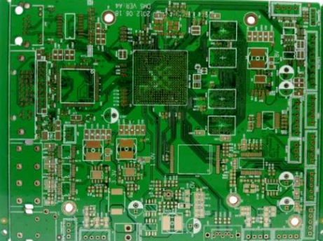
Aerospace high speed pcb design
Signal integrity issues and solutions in high-speed PCB designIn high-speed PCB design, signal integrity issues are a challenge that cannot be ignored. As the frequency and speed of electronic devices continue to increase, signal integrity issues have become more prominent.
Signal integrity issues mainly include signal reflection, crosstalk, timing error, and electromagnetic interference. These problems not only affect the transmission quality of the signal, but may also cause system function failure. Therefore, solving signal integrity issues is a key task in high-speed PCB design.
First, signal reflection is one of the common problems in high-speed PCB design.
When a signal propagates on a transmission line, if it encounters an impedance mismatch, reflection will occur. The reflected signal interferes with the original signal, causing signal distortion.
To solve this problem, designers need to ensure that the impedance of the transmission line is matched. Impedance matching can be achieved by reasonably selecting the width, thickness, and dielectric material of the transmission line.
In addition, using terminal resistors is also an effective method to absorb reflected signals and reduce signal distortion.
Secondly, crosstalk is another signal integrity issue that needs attention.
Crosstalk refers to the signal on one signal line affecting the adjacent signal line through electromagnetic coupling, resulting in signal interference. To reduce crosstalk, designers can take a variety of measures.
For example, increase the spacing between signal lines, use shielding layers or ground planes to isolate signal lines. In addition, using differential signal transmission is also an effective method. Differential signals have strong anti-interference ability and can significantly reduce the impact of crosstalk.
Timing error is another important signal integrity issue in high-speed PCB design.
Timing error refers to the error caused by the delay asynchronization during the transmission of the signal. In order to reduce the timing error, designers need to accurately control the transmission path and length of the signal.
By reasonable wiring, ensuring the symmetry and equal length of the signal path, the timing error can be effectively reduced.
In addition, using clock synchronization technology is also a common method to ensure the synchronous transmission of the signal.
Finally, electromagnetic interference is an issue that cannot be ignored in high-speed PCB design.
Electromagnetic interference not only affects the transmission quality of the signal, but may also interfere with surrounding electronic equipment. In order to reduce electromagnetic interference, designers can take a variety of measures.
For example, reasonably layout the power supply and ground planes, and use filters and decoupling capacitors to suppress high-frequency noise. In addition, using multi-layer PCB design is also an effective method to reduce electromagnetic interference by adding ground planes and shielding layers.
In summary, the signal integrity issue in high-speed PCB design is a complex and important topic. Through reasonable design and optimization, problems such as signal reflection, crosstalk, timing error and electromagnetic interference can be effectively solved, thereby improving the quality of signal transmission and the reliability of the system.
With the continuous advancement of technology, signal integrity issues will be better solved, providing a solid foundation for the development of high-speed electronic devices.
High-speed PCB Material Selection Guide in Aerospace Applications The design of high-speed printed circuit boards (PCBs) in aerospace applications is a complex and critical process.
Choosing the right material not only affects the performance of the circuit board, but is also directly related to the reliability and safety of the entire system.
First, the dielectric constant (Dk) and dissipation factor (Df) of the material are two key parameters.
The dielectric constant determines the speed of signal propagation in the material, while the dissipation factor affects the degree of signal attenuation. In high-speed applications, materials with low dielectric constants and low dissipation factors can effectively reduce signal delays and losses, thereby improving the overall performance of the system.
Next, thermal management is also a factor that cannot be ignored.
Aerospace equipment often operates under extreme temperature conditions, so PCB materials must have good thermal conductivity and thermal stability.
Materials with high thermal conductivity can quickly dissipate heat and prevent the circuit board from overheating, thereby extending the service life of the equipment. In addition, the coefficient of thermal expansion (CTE) of the material also needs to match other components to avoid mechanical stress and damage caused by thermal expansion and contraction.
In addition to electrical and thermal performance, mechanical strength and durability are also important considerations when selecting materials.
Aerospace equipment will experience severe vibration and shock during operation, so PCB materials must have high strength and impact resistance.
Glass-fiber-reinforced epoxy resins (such as FR-4) are common choices, but for more demanding applications, polyimide and ceramic-based materials may be more suitable.
In addition, environmental adaptability is also a key factor.
Aerospace equipment needs to operate in a variety of harsh environments, including high humidity, high radiation, and corrosive gases.
Therefore, PCB materials must have good moisture resistance, radiation resistance, and corrosion resistance.
Some high-performance polymers and ceramic materials perform well in these aspects and can meet stringent environmental requirements.
When selecting materials, the compatibility of the manufacturing process must also be considered. Different materials have different processing characteristics, and some high-performance materials may require special manufacturing processes and equipment, which will increase production costs and complexity.
Therefore, under the premise of meeting performance requirements, choosing materials that are easy to process and cost-controlled is also an important strategy.
In summary, high-speed PCB design in aerospace applications requires comprehensive consideration of electrical performance, thermal management, mechanical strength, environmental adaptability, and manufacturing processes.
By properly selecting and optimizing materials, the performance and reliability of the circuit board can be significantly improved, thereby ensuring the stable operation of the entire system under extreme conditions. Electromagnetic Interference Control Technology in High-Speed PCB Design
In high-speed PCB design, electromagnetic interference (EMI) control technology is an important part to ensure system performance and reliability.
As the operating frequency of electronic equipment continues to increase, the problem of electromagnetic interference becomes more and more prominent.
First of all, it is crucial to understand the source of electromagnetic interference. Electromagnetic interference mainly comes from high-frequency signals in the circuit, which will generate electromagnetic radiation on the PCB, thereby affecting the normal operation of other circuits. Therefore, designers need to take a series of measures to control and reduce electromagnetic interference.
Next, reasonable layout and wiring are one of the key steps to control electromagnetic interference. In the layout stage, designers should try to separate high-frequency signal lines from sensitive signal lines to avoid mutual interference between them. In addition, the length of the signal line should be shortened as much as possible to reduce radiation and interference during signal transmission. By optimizing layout and wiring, the risk of electromagnetic interference can be effectively reduced.
In addition, the use of appropriate shielding technology is also one of the important means to control electromagnetic interference. Shielding technology can effectively block the propagation of electromagnetic radiation by adding a metal shielding layer or shielding cover to the circuit board. Especially in high-speed PCB design, shielding technology can significantly improve the anti-interference ability of the circuit. However, the application of shielding technology needs to comprehensively consider the cost and design complexity, so it is necessary to weigh the pros and cons in actual design.
At the same time, grounding design also plays a vital role in electromagnetic interference control. A good grounding design can provide a low-impedance loop to reduce the propagation of electromagnetic interference. Designers should ensure the integrity of the grounding layer to avoid breaks or discontinuities. In addition, reasonable grounding methods, such as the combination of multi-point grounding and single-point grounding, can further improve the anti-interference ability of the circuit.
Finally, filtering technology is also one of the effective means to control electromagnetic interference. By adding filters to the circuit, high-frequency interference signals can be effectively filtered out to ensure the purity of the signal. Common filters include low-pass filters, high-pass filters, and band-pass filters. Designers should choose the appropriate filter type and parameters according to the specific circuit requirements to achieve the best interference suppression effect.
One of the common strategies is to use thermally conductive materials. These materials have high thermal conductivity and can quickly conduct heat from the heat source to the heat sink or other cooling device. Common thermal conductive materials include copper and aluminum, which not only have excellent thermal conductivity but are also easy to process and install. In addition, the selection of thermal conductive materials also needs to consider their weight and cost, especially in aerospace applications, where weight is a key factor.
Next, the thermal management strategy also includes optimizing the PCB layout. By properly arranging the location of high-power components, heat accumulation can be minimized. For example, placing high-power components at the edge of the PCB or close to the heat sink can dissipate heat more effectively. In addition, designers can also enhance the heat dissipation capacity of the PCB by adding thermal vias and heat dissipation layers. These vias and layers can increase the conduction path of heat, thereby improving the overall heat dissipation efficiency.
In addition, using active cooling systems is also an effective thermal management strategy. Active cooling systems include fans, liquid cooling systems, etc., which can remove heat through forced convection or liquid circulation. Although these systems are expensive to design and maintain, they can significantly improve the heat dissipation effect in high power density applications. However, the use of active cooling systems needs to comprehensively consider their impact on system weight, volume and power consumption.
At the same time, thermal simulation technology also plays an important role in thermal management strategies. Through thermal simulation software, designers can predict and analyze the thermal performance of PCBs during the design stage, thereby optimizing thermal management solutions.
This can not only reduce the design cycle, but also reduce the cost of trials and modifications. The application of thermal simulation technology enables designers to discover potential thermal problems at an early stage and take appropriate measures to solve them.
Finally, thermal management strategies should also include consideration of environmental conditions. In aerospace applications, electronic equipment may face extreme temperature changes and harsh working environments.
Therefore, designers need to ensure that thermal management solutions can operate effectively under various environmental conditions. This may include using high-temperature resistant materials, designing redundant heat dissipation paths, etc.
In summary, thermal management strategies in aerospace high-speed PCB design are a multi-level, multi-faceted and comprehensive process.
By rationally selecting thermal conductive materials, optimizing PCB layout, using active cooling systems, applying thermal simulation technology, and considering environmental conditions, designers can effectively solve thermal management problems and ensure that electronic equipment can operate stably under various conditions.
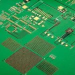
Stacking structure optimization method in high-speed PCB design
In high-speed PCB design, stacking structure optimization is an important part to ensure signal integrity and electromagnetic compatibility. First of all, the choice of stacking structure directly affects the signal transmission path and impedance control.
Through reasonable stacking design, signal reflection and crosstalk can be effectively reduced, thereby improving the overall performance of the circuit. Usually, high-speed PCB design will adopt a multi-layer board structure to better manage the relationship between the signal layer and the power layer.
Next, the arrangement order of the signal layer and the power layer is one of the key factors in the optimization of the stacking structure.
In order to reduce electromagnetic interference, the signal layer should be as close to the ground layer as possible, so that a low-impedance return path can be formed to reduce signal radiation and interference.
In addition, the distance between the power layer and the ground layer should also be shortened as much as possible to reduce power noise and power integrity issues. In this way, it can be ensured that the high-speed signal remains stable during transmission.
In addition, the symmetry of the stacking structure is also an important aspect to consider. A symmetrical stacking structure can reduce the warping and deformation of the board during manufacturing and use, thereby improving the mechanical stability and reliability of the PCB.
Especially in the aerospace field, the mechanical properties of PCBs are particularly important because they need to work in extreme environments. Therefore, when optimizing the stacking structure, designers should try to maintain the symmetry of each layer.
Further, the optimization of the stacking structure also needs to consider the routing length and path of the signal. The transmission speed of high-speed signals is very fast, and any slight path difference will cause signal delay and distortion. Therefore, when designing the stacking structure, the routing length of the high-speed signal should be equal as much as possible to reduce the delay difference of the signal.
In addition, signal routing should avoid sharp turns and crossings as much as possible to reduce signal reflection and loss.
Finally, the optimization of the stacking structure also needs to be combined with specific application requirements and design specifications. For example, in the aerospace field, high-speed PCB design not only needs to consider signal integrity and electromagnetic compatibility, but also needs to meet strict environmental requirements and reliability standards. Therefore, when optimizing the stacking structure, designers should comprehensively consider various factors to ensure that the designed PCB can work stably and reliably in practical applications.
In summary, the optimization of the stacking structure in high-speed PCB design is a complex and critical process. Through reasonable stacking design, signal integrity and electromagnetic compatibility can be effectively improved to ensure the overall performance and reliability of the circuit.