Bed of nails pcb assembly testing
Benefits Of Bed Of Nails PCB Assembly Testing
Bed of nails PCB assembly testing, also known as in-circuit testing (ICT), is a method that has gained significant traction in the electronics manufacturing industry due to its numerous benefits.
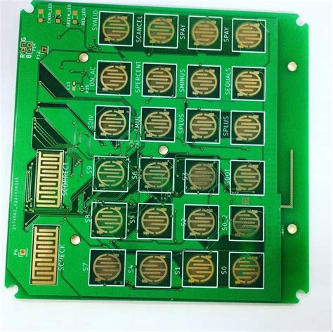
This testing technique involves the use of a fixture, often referred to as a “bed of nails,” which contains an array of spring-loaded pins. These pins make contact with specific test points on a printed circuit board (PCB) to evaluate its functionality and integrity.
The advantages of this method are manifold, making it an indispensable tool in ensuring the quality and reliability of electronic assemblies.
One of the primary benefits of bed of nails PCB assembly testing is its ability to provide comprehensive coverage. Unlike other testing methods that may only assess certain aspects of a PCB, in-circuit testing can evaluate a wide range of parameters. This includes checking for shorts, opens, resistance, capacitance, and the correct operation of active components.
By offering such extensive coverage, this method ensures that any defects or issues are identified early in the production process, thereby reducing the likelihood of faulty products reaching the end user.
Moreover, bed of nails testing is known for its high accuracy and repeatability.
The precision with which the spring-loaded pins make contact with the test points ensures that the measurements are reliable and consistent. This is particularly important in high-volume manufacturing environments where maintaining uniformity across multiple units is crucial.
The repeatability of this testing method also means that it can be used to monitor the quality of production over time, providing valuable data for process improvement and quality control.
In addition to its accuracy, bed of nails PCB assembly testing is also highly efficient.
The automated nature of this method allows for rapid testing of PCBs, significantly reducing the time required for quality assurance. This efficiency is further enhanced by the ability to test multiple points simultaneously, which is a distinct advantage over manual testing methods. Consequently, manufacturers can achieve faster turnaround times, which is essential in meeting tight production schedules and maintaining a competitive edge in the market.
Another significant benefit of bed of nails testing is its cost-effectiveness.
While the initial investment in the test fixture and setup may be substantial, the long-term savings are considerable. The ability to detect defects early in the production process means that rework and scrap costs are minimized. Furthermore, the high throughput and reduced labor costs associated with automated testing contribute to overall cost savings. This makes bed of nails testing an economically viable option for manufacturers aiming to optimize their production processes.
Furthermore, the versatility of bed of nails PCB assembly testing cannot be overlooked.
This method can be adapted to test a wide variety of PCB designs and configurations, making it suitable for diverse applications across different industries. Whether it is consumer electronics, automotive systems, or medical devices, the adaptability of this testing technique ensures that it can meet the specific requirements of various sectors.
In conclusion, the benefits of bed of nails PCB assembly testing are extensive and multifaceted. Its comprehensive coverage, high accuracy, efficiency, cost-effectiveness, and versatility make it an invaluable tool in the electronics manufacturing industry. By ensuring the quality and reliability of PCBs, this testing method not only enhances product performance but also contributes to customer satisfaction and brand reputation. As technology continues to evolve, the importance of robust testing methods like bed of nails will only become more pronounced, underscoring its critical role in the future of electronics manufacturing.
How To Design A Bed Of Nails Fixture For PCB Testing
Designing a bed of nails fixture for PCB testing is a meticulous process that requires a deep understanding of both the mechanical and electrical aspects of printed circuit boards (PCBs). The bed of nails fixture, also known as a test fixture, is an essential tool in the electronics manufacturing industry, used to ensure the functionality and reliability of PCBs before they are integrated into final products. To design an effective bed of nails fixture, one must consider several critical factors, including the layout of the PCB, the type of tests to be conducted, and the specific requirements of the testing environment.
Initially, it is crucial to analyze the PCB layout thoroughly.
This involves examining the placement of components, the routing of traces, and the location of test points. The test points are specific locations on the PCB where electrical connections can be made to measure various parameters such as voltage, current, and signal integrity. These points must be accessible and clearly marked to facilitate accurate testing. Additionally, the spacing between test points should be sufficient to prevent short circuits and ensure reliable contact with the test probes.
Once the PCB layout has been analyzed, the next step is to determine the type of tests that will be conducted.
Common tests include continuity testing, which checks for open or short circuits; functional testing, which verifies the operation of the PCB under normal conditions; and in-circuit testing, which measures the performance of individual components. Each type of test may require different configurations of the bed of nails fixture, so it is essential to define the testing requirements clearly at the outset.
With the testing requirements in mind, the design of the bed of nails fixture can begin.
The fixture typically consists of a base plate, a set of spring-loaded test probes, and a mechanism to hold the PCB in place. The base plate is usually made of a durable material such as aluminum or fiberglass, which provides a stable platform for the test probes. The test probes, also known as pogo pins, are arranged in a pattern that matches the layout of the test points on the PCB. These probes are designed to make reliable electrical contact with the test points when the PCB is pressed onto the fixture.
To ensure accurate and repeatable testing, the mechanism that holds the PCB in place must be carefully designed. This mechanism often includes a clamping system that secures the PCB firmly against the test probes, ensuring consistent contact pressure. Additionally, alignment features such as guide pins or slots may be incorporated to ensure that the PCB is positioned correctly on the fixture. These alignment features are particularly important for high-density PCBs, where the spacing between test points is minimal.
Furthermore, it is important to consider the electrical characteristics of the test probes and the connections to the testing equipment.
The probes must have low contact resistance to ensure accurate measurements, and the connections to the testing equipment should be designed to minimize signal degradation. Shielded cables and connectors may be used to reduce electromagnetic interference and ensure the integrity of the test signals.
In conclusion, designing a bed of nails fixture for PCB testing is a complex process that requires careful consideration of the PCB layout, testing requirements, and mechanical and electrical design aspects. By thoroughly analyzing these factors and incorporating precise alignment and secure clamping mechanisms, one can create a reliable and effective test fixture that ensures the functionality and reliability of PCBs in the manufacturing process.
Common Challenges In Bed Of Nails PCB Testing And Solutions
Bed of nails PCB assembly testing is a widely used method for ensuring the functionality and reliability of printed circuit boards (PCBs). However, this testing technique is not without its challenges. Understanding these common issues and their solutions is crucial for optimizing the testing process and ensuring high-quality PCB production.
One of the primary challenges in bed of nails PCB testing is the alignment of the test fixture with the PCB.
Misalignment can lead to inaccurate test results or even damage to the board. This issue often arises due to variations in PCB dimensions or warping during the manufacturing process. To address this, manufacturers can implement precise alignment mechanisms and regularly calibrate their equipment. Additionally, using high-quality materials for the test fixture can minimize wear and tear, ensuring consistent alignment over time.
Another significant challenge is the contact reliability between the test probes and the PCB pads.
Poor contact can result in false negatives, where a functional board is incorrectly identified as faulty. This problem is often exacerbated by the presence of contaminants such as flux residues or oxidation on the PCB pads. To mitigate this, thorough cleaning of the PCB before testing is essential. Employing gold-plated test probes can also enhance contact reliability, as gold is highly resistant to oxidation and provides a more consistent connection.
The complexity of modern PCBs, with their high component density and fine pitch, presents another hurdle in bed of nails testing.
As PCBs become more intricate, the number of test points increases, making it challenging to design a test fixture that can accommodate all necessary connections without causing interference. To overcome this, manufacturers can use advanced fixture design software that optimizes the placement of test probes. Additionally, modular test fixtures can be employed, allowing for easy reconfiguration to accommodate different PCB designs.
Signal integrity is another critical concern in bed of nails PCB testing.
High-speed signals can be distorted by the test fixture, leading to inaccurate measurements. This issue is particularly relevant for PCBs used in high-frequency applications such as telecommunications and computing. To address signal integrity issues, manufacturers can use impedance-controlled test probes and fixtures. Additionally, incorporating shielding and proper grounding techniques can help minimize signal interference and ensure accurate test results.
Mechanical stress on the PCB during testing is another challenge that cannot be overlooked.
The pressure exerted by the test probes can cause damage to delicate components or even lead to board warping. To mitigate this risk, manufacturers can use spring-loaded test probes that apply consistent, controlled pressure. Furthermore, designing the test fixture to distribute the force evenly across the PCB can help prevent localized stress and potential damage.
Finally, the cost and time associated with bed of nails PCB testing can be significant, particularly for small production runs or prototypes. The initial setup of the test fixture can be time-consuming and expensive. To address this, manufacturers can consider using alternative testing methods such as flying probe testing for low-volume production. Flying probe testing offers greater flexibility and lower setup costs, although it may not be as fast or comprehensive as bed of nails testing for high-volume production.
In conclusion, while bed of nails PCB assembly testing presents several challenges, understanding and addressing these issues can lead to more reliable and efficient testing processes. By focusing on alignment, contact reliability, fixture design, signal integrity, mechanical stress, and cost considerations, manufacturers can optimize their testing procedures and ensure the production of high-quality PCBs.
Comparing Bed Of Nails Testing To Other PCB Testing Methods
In the realm of printed circuit board (PCB) assembly testing, various methodologies are employed to ensure the reliability and functionality of the final product. Among these, the bed of nails testing method stands out due to its unique approach and specific advantages. However, to fully appreciate its value, it is essential to compare it with other prevalent PCB testing methods, such as in-circuit testing (ICT), functional testing, and flying probe testing.
The bed of nails testing method involves a fixture with numerous spring-loaded pins, each corresponding to a specific test point on the PCB.
When the PCB is placed on this fixture, the pins make contact with the test points, allowing for simultaneous testing of multiple connections and components. This method is particularly advantageous for high-volume production runs due to its speed and efficiency. The ability to test numerous points concurrently significantly reduces the time required for each PCB, making it a cost-effective solution for large-scale manufacturing.
In contrast, in-circuit testing (ICT) also aims to verify the functionality of individual components and connections on a PCB. However, ICT typically uses a combination of electrical probes and software to perform these tests. While ICT can be highly effective, it often requires more time per board compared to the bed of nails method, especially when dealing with complex PCBs with numerous components. Additionally, ICT setups can be more expensive due to the need for sophisticated software and hardware integration.
Functional testing, another common method, focuses on evaluating the overall performance of the PCB within its intended application.
This approach involves simulating the operational environment and conditions to ensure that the PCB performs as expected. While functional testing provides a comprehensive assessment of the PCB’s performance, it is generally more time-consuming and less suited for identifying specific component-level issues. Consequently, it is often used in conjunction with other testing methods, such as bed of nails or ICT, to provide a more complete evaluation.
Flying probe testing offers a different approach by using movable probes to test individual points on the PCB.
This method is highly flexible and does not require a custom fixture, making it ideal for low-volume production runs or prototype testing. However, the sequential nature of flying probe testing means that it is generally slower than the bed of nails method, particularly for complex PCBs with many test points. Additionally, while flying probe testing can be highly accurate, it may not be as effective for high-density boards where access to test points is limited.
When comparing these methods, it becomes clear that each has its own set of strengths and limitations.
The bed of nails testing method excels in high-speed, high-volume production environments due to its ability to test multiple points simultaneously. In-circuit testing offers a balance of thoroughness and efficiency but may be more costly and time-consuming for complex boards. Functional testing provides a holistic view of the PCB’s performance but is less effective for pinpointing specific issues. Flying probe testing offers flexibility and precision but is generally slower and less suited for high-density boards.
Ultimately, the choice of testing method depends on various factors, including production volume, PCB complexity, and specific testing requirements. In many cases, a combination of methods may be employed to achieve the most comprehensive and efficient testing process. By understanding the unique advantages and limitations of each method, manufacturers can make informed decisions to ensure the reliability and functionality of their PCBs, thereby enhancing the overall quality of their products.