Diy multilayer pcb
Step-by-Step Guide to Designing Your Own Multilayer PCB
Designing your own multilayer printed circuit board (PCB) can be a rewarding endeavor, offering both the satisfaction of creating a custom solution and the potential for significant cost savings. To embark on this journey, it is essential to understand the step-by-step process involved in creating a multilayer PCB, from initial design to final production. This guide aims to provide a comprehensive overview of the necessary steps, ensuring a smooth and successful project.
The first step in designing a multilayer PCB is to conceptualize your circuit.
Begin by defining the requirements and specifications of your project, including the number of layers needed, the types of components to be used, and the overall dimensions of the board. Once you have a clear understanding of your project’s needs, you can proceed to create a schematic diagram. This diagram serves as a blueprint for your PCB, detailing the connections between various components and ensuring that the circuit functions as intended.
With the schematic diagram in hand, the next step is to select a PCB design software.
There are numerous options available, ranging from free, open-source programs to professional-grade tools. Choose a software that best suits your needs and expertise level. Once you have selected your software, import your schematic diagram and begin the process of laying out the PCB. This involves placing components on the board and routing the electrical connections between them. It is crucial to pay attention to the placement of components and the routing of traces, as these factors can significantly impact the performance and reliability of your PCB.
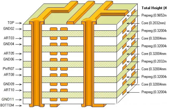
As you design your multilayer PCB, it is important to consider the stack-up configuration.
The stack-up refers to the arrangement of the various layers within the PCB, including signal layers, power planes, and ground planes. A well-designed stack-up can help minimize electromagnetic interference (EMI) and improve signal integrity. Typically, a four-layer PCB consists of two signal layers sandwiched between a power plane and a ground plane. However, more complex designs may require additional layers to accommodate intricate routing and power distribution requirements.
Once the layout and stack-up are finalized, the next step is to generate the necessary files for manufacturing.
These files, commonly referred to as Gerber files, contain all the information required by a PCB manufacturer to produce your board. Ensure that you thoroughly review and verify these files before sending them to the manufacturer, as any errors or discrepancies can lead to costly delays and rework.
After submitting your Gerber files to a PCB manufacturer, the production process begins.
This typically involves several stages, including the fabrication of individual layers, the alignment and lamination of these layers, and the drilling of vias and holes. Once the board is assembled, it undergoes a series of inspections and tests to ensure that it meets the required specifications and quality standards.
Upon receiving your completed multilayer PCB, the final step is to assemble and test your circuit.
Carefully solder the components onto the board, following the layout specified in your design. Once all components are in place, perform a series of tests to verify that the circuit functions as intended. This may include continuity checks, signal integrity tests, and functional testing of the overall system.
In conclusion, designing your own multilayer PCB involves a series of well-defined steps, from initial concept and schematic creation to layout design, manufacturing, and final assembly. By following this guide and paying close attention to detail at each stage, you can successfully create a custom multilayer PCB that meets your project’s requirements and delivers reliable performance.
Essential Tools and Materials for DIY Multilayer PCB Projects
Creating a DIY multilayer printed circuit board (PCB) is a complex yet rewarding endeavor that requires a precise set of tools and materials. Understanding the essential components and equipment needed for such a project is crucial for achieving a successful outcome. To begin with, one must have a clear design plan, typically created using PCB design software such as Eagle, KiCad, or Altium Designer. These programs allow for the meticulous planning of each layer, ensuring that all connections and components are accurately represented.
Once the design is finalized, the next step involves transferring the design onto the PCB material.
For this, a high-quality laser printer is indispensable, as it is used to print the design onto a special transfer paper. This paper will later be used to transfer the design onto the copper-clad board. Additionally, a laminator or a clothes iron is necessary to apply heat and pressure, ensuring that the toner from the transfer paper adheres properly to the copper surface.
After the design has been successfully transferred, the etching process begins.
This requires a suitable etching solution, commonly ferric chloride or ammonium persulfate, to remove the excess copper from the board, leaving only the desired circuit pattern. It is important to handle these chemicals with care, using appropriate safety gear such as gloves and goggles, and working in a well-ventilated area to avoid inhaling any harmful fumes.
For multilayer PCBs, the process involves additional steps to align and bond multiple layers.
This necessitates the use of alignment pins or a registration system to ensure that all layers are perfectly aligned before bonding. A hydraulic press or a vacuum laminator is often employed to apply uniform pressure and heat, effectively bonding the layers together. This step is critical, as any misalignment can result in faulty connections and a non-functional PCB.
Drilling precise holes for vias and through-hole components is another essential task.
A high-speed PCB drill or a CNC machine is typically used for this purpose, as it provides the accuracy and precision required for such intricate work. The holes must be plated to establish electrical connections between the layers, a process that can be achieved through electroplating or by using conductive ink.
Soldering is the final step in assembling the PCB.
A high-quality soldering iron with a fine tip is necessary for attaching components to the board. Additionally, solder paste and a reflow oven may be used for surface-mount components, ensuring a clean and reliable connection. It is also advisable to have a multimeter on hand to test the continuity and functionality of the circuit before powering it up.
In conclusion, embarking on a DIY multilayer PCB project requires a comprehensive understanding of the tools and materials involved. From design software and transfer methods to etching solutions and drilling equipment, each component plays a vital role in the successful creation of a multilayer PCB. By meticulously following each step and utilizing the appropriate tools, one can achieve a functional and reliable multilayer PCB, paving the way for innovative electronic projects.

Common Mistakes to Avoid When Creating Multilayer PCBs at Home
Creating multilayer printed circuit boards (PCBs) at home can be a rewarding yet challenging endeavor. While the process allows for greater customization and control over the final product, it also presents numerous opportunities for errors.
Understanding common mistakes and how to avoid them is crucial for achieving a successful outcome.
One of the most frequent errors is inadequate planning. Before diving into the fabrication process, it is essential to meticulously design the PCB layout using specialized software. Neglecting this step can lead to misaligned layers, which can compromise the functionality of the entire board. Therefore, investing time in thorough planning and double-checking the design can save significant effort and resources in the long run.
Another common mistake is improper material selection.
The choice of substrate, copper thickness, and dielectric materials can significantly impact the performance of the PCB. Using substandard materials can result in poor electrical performance and reduced durability. It is advisable to research and select high-quality materials that meet the specific requirements of your project. Additionally, ensuring that all materials are compatible with each other is vital to prevent issues such as delamination or warping during the manufacturing process.
Transitioning to the actual fabrication, one must be cautious about the etching process.
Over-etching or under-etching can lead to incomplete or excessive removal of copper, which can affect the circuit’s integrity. To avoid this, it is important to carefully monitor the etching time and use the appropriate etching solution. Consistency in the etching process can be achieved by maintaining a controlled environment and following the recommended guidelines for the chemicals used.
Furthermore, layer alignment is a critical aspect that requires precision.
Misalignment of layers can cause short circuits or open circuits, rendering the PCB non-functional. To ensure proper alignment, it is beneficial to use alignment pins or registration marks during the lamination process. This practice helps in maintaining the correct positioning of each layer, thereby enhancing the overall reliability of the PCB.
Soldering is another area where mistakes are commonly made.
Poor soldering techniques can lead to weak joints, which can cause intermittent connections or complete failure of the circuit. It is essential to use the right type of solder and flux, and to apply the correct amount of heat. Practicing good soldering habits, such as cleaning the soldering iron tip regularly and avoiding excessive solder, can significantly improve the quality of the connections.
In addition to these technical aspects, safety should never be overlooked.
Handling chemicals and high-temperature equipment poses risks that can be mitigated by following proper safety protocols. Wearing protective gear, working in a well-ventilated area, and being aware of emergency procedures are fundamental practices that ensure a safe working environment.
Lastly, testing and troubleshooting are indispensable steps in the PCB creation process.
Skipping these steps can result in undetected issues that may only surface during the operation of the final product. Conducting thorough testing using multimeters, oscilloscopes, and other diagnostic tools can help identify and rectify any faults before the PCB is put to use.
In conclusion, creating multilayer PCBs at home involves a series of intricate steps that require careful attention to detail. By avoiding common mistakes such as inadequate planning, improper material selection, inconsistent etching, misalignment of layers, poor soldering techniques, neglecting safety measures, and skipping testing, one can significantly enhance the chances of producing a functional and reliable PCB. Through meticulous preparation and adherence to best practices, the complexities of DIY multilayer PCB fabrication can be effectively managed, leading to successful project outcomes.
Advanced Techniques for DIY Multilayer PCB Fabrication
Creating a multilayer printed circuit board (PCB) at home can be a challenging yet rewarding endeavor for electronics enthusiasts and professionals alike. The process involves several advanced techniques that require precision, patience, and a thorough understanding of PCB design principles. To begin with, it is essential to have a clear and detailed design of the PCB, typically created using specialized software such as Eagle, KiCad, or Altium Designer. These tools allow for the meticulous planning of each layer, ensuring that signal integrity and electrical performance are maintained.
Once the design is finalized, the next step involves the preparation of the individual layers.
This process starts with the selection of appropriate materials, usually copper-clad laminates, which serve as the foundation for each layer. The copper is then etched to create the desired circuit patterns. This can be achieved through various methods, including photoresist techniques, where a photosensitive material is applied to the copper surface and exposed to UV light through a mask of the circuit design. The exposed areas are then developed and etched away, leaving behind the copper traces.
After the individual layers are prepared, the next critical step is the alignment and lamination of these layers.
Proper alignment is crucial to ensure that the vias, or vertical interconnect accesses, line up correctly between layers. This is typically done using alignment pins or optical alignment systems. The layers are then laminated together under high pressure and temperature, using a prepreg material that acts as an adhesive. This process not only bonds the layers together but also ensures the mechanical stability and electrical insulation between them.
Drilling the vias is another essential step in the fabrication of multilayer PCBs.
Precision drilling equipment, often CNC machines, are used to create the holes that will later be plated to form electrical connections between the layers. The accuracy of this step is paramount, as any misalignment can lead to faulty connections and compromised functionality of the PCB.
Following the drilling process, the vias are plated with copper to establish the necessary electrical connections.
This is typically done through an electroplating process, where the PCB is submerged in a copper sulfate solution and an electric current is applied. The copper ions in the solution are deposited onto the walls of the drilled holes, creating a conductive path between the layers.
The final steps in the DIY multilayer PCB fabrication process involve the application of a solder mask and the addition of surface finishes.
The solder mask, usually a green epoxy, is applied to protect the copper traces from oxidation and to prevent solder bridges during component assembly. Surface finishes, such as HASL (Hot Air Solder Leveling), ENIG (Electroless Nickel Immersion Gold), or OSP (Organic Solderability Preservatives), are then applied to the exposed copper pads to enhance solderability and protect against corrosion.
In conclusion, fabricating a multilayer PCB at home requires a combination of advanced techniques and meticulous attention to detail. From the initial design and material preparation to the alignment, lamination, drilling, and finishing processes, each step plays a crucial role in ensuring the functionality and reliability of the final product. While challenging, mastering these techniques can significantly enhance one’s ability to create complex and high-performance electronic circuits, opening up new possibilities for innovation and experimentation in the field of electronics.