Etching pcb manufacturing
Introduction To Etching PCB Manufacturing
Printed Circuit Boards (PCBs) are the backbone of modern electronic devices, serving as the platform upon which electronic components are mounted and interconnected.
One of the most critical steps in PCB manufacturing is the etching process
which involves the removal of unwanted copper from a copper-clad laminate to create the desired circuit patterns. This process is fundamental to ensuring the functionality and reliability of the final product. Understanding the various etching techniques employed in PCB manufacturing is essential for anyone involved in the design and production of electronic devices.
The etching process begins with the preparation of the copper-clad laminate, which is typically coated with a photosensitive resist material.
This resist material is then exposed to ultraviolet (UV) light through a photomask that contains the desired circuit pattern. The areas of the resist exposed to UV light harden, while the unexposed areas remain soft and can be easily removed. This step, known as photolithography, creates a protective layer that defines the areas of copper to be retained.
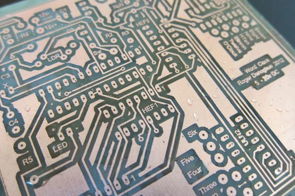
Following photolithography, the PCB undergoes the actual etching process.
One of the most common etching techniques is chemical etching, which involves immersing the PCB in a solution of ferric chloride or ammonium persulfate. These chemicals react with the exposed copper, dissolving it and leaving behind the desired circuit pattern. Chemical etching is widely used due to its simplicity and cost-effectiveness. However, it requires careful control of the etching time and solution concentration to ensure precise results.
In addition to chemical etching, there are other techniques such as plasma etching and laser etching.
Plasma etching utilizes ionized gas to remove the unwanted copper. This method offers high precision and is particularly useful for creating fine features and intricate patterns. However, it requires specialized equipment and is generally more expensive than chemical etching. Laser etching, on the other hand, employs a focused laser beam to vaporize the unwanted copper. This technique provides excellent accuracy and is ideal for prototyping and small-scale production. Nevertheless, it is not as widely adopted for large-scale manufacturing due to its higher cost and slower processing speed.
Another important aspect of the etching process is the removal of the resist material after etching.
This step, known as stripping, involves using a solvent or alkaline solution to dissolve the hardened resist, revealing the final copper circuit pattern. Proper stripping is crucial to ensure that no resist residues remain, which could interfere with subsequent manufacturing steps such as soldering and component placement.
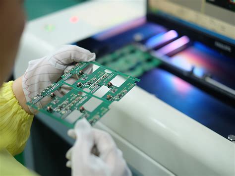
Quality control is an integral part of the etching process.
Inspection techniques such as optical microscopy and automated optical inspection (AOI) are employed to detect any defects or inconsistencies in the etched patterns. These inspections help identify issues such as under-etching, over-etching, and incomplete resist removal, which can affect the performance and reliability of the PCB.
In conclusion, etching is a vital step in PCB manufacturing that requires careful attention to detail and precise control of various parameters. The choice of etching technique depends on factors such as the complexity of the circuit design, production volume, and cost considerations. By understanding the different etching methods and their respective advantages and limitations, manufacturers can optimize their processes to produce high-quality PCBs that meet the stringent demands of modern electronic devices.
Benefits Of Using Ferric Chloride For PCB Etching
Ferric chloride, a chemical compound with the formula FeCl3, is widely recognized for its efficacy in the etching process of printed circuit boards (PCBs). This etching agent offers numerous benefits that make it a preferred choice among professionals in the electronics manufacturing industry.
One of the primary advantages of using ferric chloride for PCB etching is its high etching precision.
The compound reacts effectively with the copper layer on the PCB, dissolving it to create intricate circuit patterns with remarkable accuracy. This precision is crucial for the development of high-quality electronic devices, where even minor deviations can lead to significant performance issues.
Moreover, ferric chloride is known for its cost-effectiveness.
Compared to other etching agents, it is relatively inexpensive and readily available, making it an economical option for both small-scale and large-scale PCB manufacturing. This affordability does not compromise its effectiveness, as ferric chloride consistently delivers reliable results. Additionally, the compound’s long shelf life ensures that it remains potent over extended periods, reducing the need for frequent replacements and further contributing to cost savings.
Another significant benefit of ferric chloride is its ease of use.
The etching process with ferric chloride is straightforward, requiring minimal specialized equipment. This simplicity allows manufacturers to integrate the etching process seamlessly into their production lines without the need for extensive modifications or additional training for personnel. Furthermore, the process can be easily scaled up or down, accommodating various production volumes and enabling manufacturers to meet diverse market demands efficiently.
Environmental considerations also play a crucial role in the selection of etching agents.
Ferric chloride, when handled and disposed of properly, poses minimal environmental risks. The compound can be neutralized with basic solutions, such as sodium hydroxide, to form non-toxic byproducts that can be safely disposed of. This aspect is particularly important in today’s manufacturing landscape, where sustainability and environmental responsibility are increasingly prioritized.
In addition to its environmental benefits,
ferric chloride offers excellent compatibility with various PCB materials. It works effectively with different types of copper-clad laminates, including those used in high-frequency and high-temperature applications. This versatility ensures that manufacturers can use ferric chloride across a wide range of projects, enhancing its utility and appeal.
Furthermore, the use of ferric chloride in PCB etching contributes to improved production efficiency.
The compound’s rapid reaction time allows for quicker etching processes, reducing overall production cycles and increasing throughput. This efficiency is vital in the competitive electronics industry, where time-to-market can significantly impact a company’s success.
Lastly, the consistency of results achieved with ferric chloride cannot be overstated.
The compound’s stable chemical properties ensure uniform etching across the entire PCB surface, minimizing defects and enhancing the reliability of the final product. This consistency is essential for maintaining high standards of quality and performance in electronic devices.
In conclusion, the benefits of using ferric chloride for PCB etching are manifold. Its high precision, cost-effectiveness, ease of use, environmental compatibility, material versatility, production efficiency, and consistent results make it an invaluable tool in the electronics manufacturing industry. As technology continues to advance, the role of ferric chloride in producing high-quality PCBs will undoubtedly remain significant, supporting the development of innovative electronic devices that drive progress and improve our daily lives.
Step-By-Step Guide To DIY PCB Etching At Home
Creating your own printed circuit boards (PCBs) at home can be a rewarding and cost-effective way to bring your electronic projects to life. The process of etching PCBs involves several meticulous steps, each requiring careful attention to detail to ensure a successful outcome. This guide will walk you through the step-by-step process of DIY PCB etching, providing you with the knowledge needed to produce high-quality boards in the comfort of your own home.
To begin with, the first step in the PCB etching process is designing your circuit.
Using software such as Eagle, KiCad, or Fritzing, you can create a schematic and layout for your PCB. Once your design is complete, print the layout onto a transparency film using a laser printer. It is crucial to ensure that the printout is of high quality, as any imperfections can affect the final etching.
Next, prepare the copper-clad board, which will serve as the base for your PCB.
Clean the board thoroughly with a fine abrasive pad or steel wool to remove any oxidation and ensure a smooth surface. This step is essential for the successful transfer of the printed design onto the board. After cleaning, rinse the board with water and dry it completely.
Following the preparation of the copper-clad board, the next step is to transfer the printed design onto the board.
This can be achieved using the toner transfer method. Place the printed transparency film onto the copper-clad board, ensuring that it is correctly aligned. Use a hot iron to press the film onto the board, applying even pressure and heat for several minutes. The heat will cause the toner to adhere to the copper surface, creating a resist that will protect the copper during the etching process.
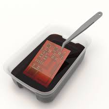
Once the design has been successfully transferred, it is time to etch the board. Prepare an etching solution by mixing ferric chloride with water in a plastic container.
Carefully submerge the copper-clad board into the solution, ensuring that it is fully covered. Gently agitate the container to help the etching process. The ferric chloride will dissolve the exposed copper, leaving only the areas protected by the toner. This step requires patience, as the etching process can take anywhere from 10 to 30 minutes, depending on the concentration of the solution and the thickness of the copper.
After the etching is complete, remove the board from the solution and rinse it thoroughly with water to stop the etching process. Use acetone or a similar solvent to remove the toner from the board, revealing the copper traces of your circuit. Inspect the board carefully to ensure that all unwanted copper has been removed and that the traces are intact.
The final step in the DIY PCB etching process is drilling holes for the components.
Using a small drill bit, carefully drill holes at the designated points on the board. This step requires precision, as any misalignment can affect the functionality of the circuit. Once the holes are drilled, you can proceed to solder the components onto the board, completing your DIY PCB.
In conclusion, etching PCBs at home involves a series of detailed steps, from designing the circuit to transferring the design, etching the board, and drilling holes for components. By following this step-by-step guide, you can create high-quality PCBs for your electronic projects, gaining both practical skills and a deeper understanding of the manufacturing process.
Common Mistakes To Avoid In PCB Etching Process
In the intricate process of etching printed circuit boards (PCBs), precision and attention to detail are paramount. However, even seasoned professionals can fall prey to common mistakes that can compromise the integrity and functionality of the final product. Understanding these pitfalls and how to avoid them is crucial for anyone involved in PCB manufacturing.
One of the most prevalent mistakes in PCB etching is inadequate cleaning of the copper-clad board before the etching process begins.
Any residual grease, dust, or fingerprints can interfere with the etching solution, leading to incomplete or uneven etching. To mitigate this, it is essential to thoroughly clean the board using appropriate solvents and ensure it is completely dry before proceeding. This step, though seemingly minor, lays the foundation for a successful etching process.
Another frequent error is the improper application of the photoresist layer.
The photoresist serves as a protective barrier that defines the areas to be etched away. If applied unevenly or with air bubbles, it can result in defects on the PCB. To avoid this, one must ensure a uniform coating by using a clean, dust-free environment and following the manufacturer’s guidelines meticulously. Additionally, allowing the photoresist to cure properly before exposure is critical to achieving a high-quality etch.
Transitioning to the exposure phase, incorrect exposure times can also lead to significant issues.
Overexposure or underexposure of the photoresist can cause the desired pattern to be inaccurately transferred onto the board. It is vital to calibrate the exposure time based on the specific photoresist and light source being used. Conducting test exposures on scrap material can help determine the optimal exposure time, thereby preventing costly mistakes on the actual PCB.
Furthermore, the etching solution itself must be carefully managed.
The concentration and temperature of the etchant play a crucial role in the etching process. A solution that is too weak or too strong can lead to under-etching or over-etching, respectively. Regularly monitoring and adjusting the etchant concentration, as well as maintaining a consistent temperature, are essential practices. Employing agitation techniques can also ensure that the etchant uniformly contacts the board, promoting even etching.
In addition to these technical aspects, handling the PCB during and after the etching process requires caution.
Mishandling can cause physical damage or contamination, which can affect the board’s performance. Using appropriate tools and handling techniques, such as wearing gloves and using non-metallic tweezers, can help prevent such issues.
Moreover, post-etching inspection is a critical step that should not be overlooked.
Carefully examining the etched board for any defects, such as incomplete etching or unintended connections, allows for timely corrections. Utilizing magnification tools and testing equipment can aid in identifying and addressing any anomalies before proceeding to the next stages of PCB manufacturing.
In conclusion, while the PCB etching process is fraught with potential pitfalls, awareness and adherence to best practices can significantly mitigate these risks. By ensuring thorough cleaning, proper application of photoresist, accurate exposure times, careful management of the etching solution, and meticulous handling and inspection, one can achieve high-quality PCBs that meet the desired specifications. Avoiding these common mistakes not only enhances the efficiency of the manufacturing process but also ensures the reliability and performance of the final product.