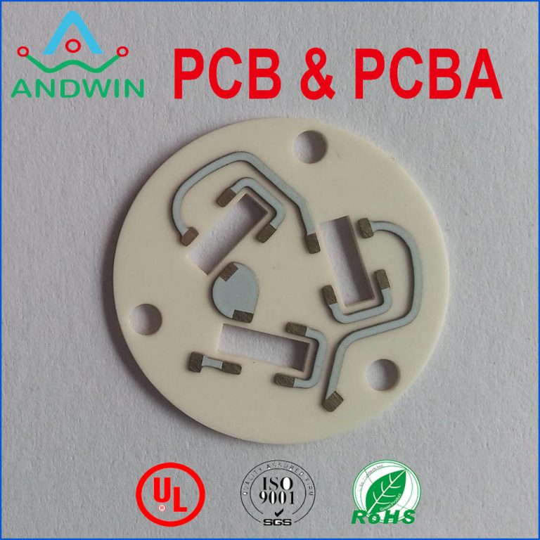
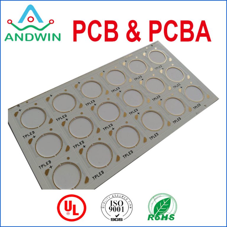
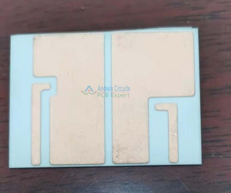
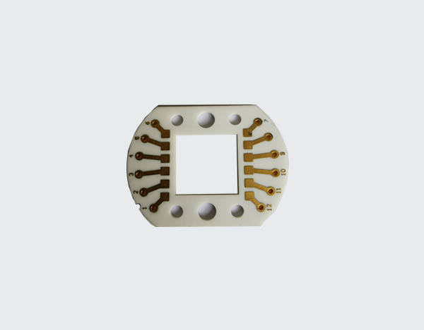
Ceramic pcb prototype
Advantages Of Using Ceramic PCB Prototypes In High-Frequency Applications
Ceramic PCB prototypes have emerged as a pivotal component in the realm of high-frequency applications, offering a multitude of advantages that make them indispensable in various advanced technological fields.
One of the primary benefits of ceramic PCBs is their exceptional thermal conductivity.
Unlike traditional FR4 boards, ceramic substrates such as aluminum oxide (Al2O3) and aluminum nitride (AlN) can efficiently dissipate heat, thereby ensuring the stability and longevity of electronic components. This characteristic is particularly crucial in high-frequency applications where excessive heat generation can lead to performance degradation and potential failure of the system.
In addition to superior thermal management, ceramic PCBs exhibit remarkable electrical insulation properties.
The high dielectric strength of ceramic materials minimizes the risk of electrical breakdown, which is essential for maintaining signal integrity in high-frequency circuits. This attribute is further complemented by the low dielectric constant and low loss tangent of ceramics, which contribute to reduced signal loss and enhanced performance. Consequently, ceramic PCBs are highly suitable for applications such as RF modules, microwave circuits, and high-power LED lighting, where maintaining signal fidelity is paramount.
Moreover, the mechanical robustness of ceramic PCBs cannot be overstated.
These substrates are inherently resistant to mechanical stress, vibration, and environmental factors such as moisture and chemical exposure. This durability ensures that ceramic PCBs can withstand harsh operating conditions, making them ideal for aerospace, automotive, and military applications. The ability to maintain structural integrity under extreme conditions not only enhances the reliability of the electronic devices but also extends their operational lifespan.
Another significant advantage of ceramic PCB prototypes is their compatibility with advanced manufacturing techniques.
The precision and versatility of ceramic materials allow for the integration of fine-pitch components and complex circuit designs. This capability is particularly beneficial in the miniaturization of electronic devices, where space constraints necessitate the use of compact and densely packed circuits. Furthermore, ceramic PCBs can be fabricated using various methods such as thick-film, thin-film, and low-temperature co-fired ceramic (LTCC) technologies, providing designers with a wide range of options to meet specific application requirements.
Transitioning to the aspect of environmental sustainability, ceramic PCBs offer an eco-friendly alternative to traditional substrates.
The production process of ceramic materials involves fewer hazardous chemicals and generates less waste, contributing to a reduced environmental footprint. Additionally, the long lifespan and high reliability of ceramic PCBs mean that electronic devices require less frequent replacement, thereby reducing electronic waste. This aligns with the growing emphasis on sustainable practices within the electronics industry.
In conclusion, the advantages of using ceramic PCB prototypes in high-frequency applications are manifold. Their superior thermal conductivity, excellent electrical insulation properties, mechanical robustness, compatibility with advanced manufacturing techniques, and environmental sustainability collectively make them an optimal choice for a wide range of advanced technological applications. As the demand for high-performance and reliable electronic devices continues to escalate, the adoption of ceramic PCBs is poised to become increasin
Step-By-Step Guide To Designing A Ceramic PCB Prototype
Designing a ceramic PCB prototype involves a series of meticulous steps that require precision and a deep understanding of both the materials and the processes involved. The journey begins with the conceptualization of the circuit design, where the specific requirements and functionalities of the PCB are outlined. This initial phase is crucial as it sets the foundation for the entire project. Engineers and designers collaborate to create a schematic diagram that represents the electrical connections and components of the circuit. This schematic serves as a blueprint for the subsequent stages of the design process.
Once the schematic is finalized, the next step is to translate this diagram into a layout design.
This involves placing the components on the ceramic substrate and routing the electrical connections between them. The choice of ceramic as a substrate material is driven by its superior thermal conductivity, mechanical strength, and electrical insulation properties, which make it ideal for high-performance and high-reliability applications. During the layout design phase, careful consideration is given to factors such as component placement, signal integrity, and thermal management to ensure optimal performance of the PCB.
Following the layout design, the focus shifts to the preparation of the ceramic substrate.
This involves selecting the appropriate type of ceramic material, such as alumina or aluminum nitride, based on the specific requirements of the application. The ceramic substrate is then cut to the desired size and shape using precision cutting tools. Surface preparation is also a critical step, as it ensures proper adhesion of the conductive traces and components to the substrate. This typically involves cleaning the surface to remove any contaminants and applying a thin layer of adhesion promoter.
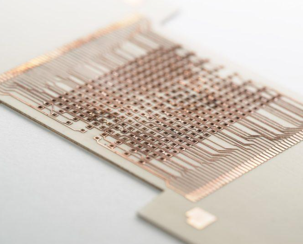
With the substrate prepared, the next step is to apply the conductive traces.
This is typically done using a screen-printing process, where a conductive paste, often made of silver or gold, is applied to the substrate through a stencil. The paste is then cured at high temperatures to form solid conductive traces. This process may be repeated multiple times to build up the required thickness of the traces. In some cases, additional layers of dielectric material may be applied between the conductive layers to create a multi-layer PCB.
Once the conductive traces are in place, the components are mounted onto the substrate.
This is typically done using a combination of surface-mount technology (SMT) and through-hole technology, depending on the type and size of the components. The components are carefully placed on the substrate and soldered in place using a reflow soldering process. This involves heating the assembly to a temperature that melts the solder, creating a strong electrical and mechanical bond between the components and the substrate.
After the components are mounted, the PCB undergoes a series of inspections and tests to ensure its functionality and reliability.
This includes visual inspections to check for any defects or misalignments, as well as electrical tests to verify the continuity and performance of the circuit. Any issues identified during this phase are addressed through rework or adjustments to the design.
Finally, the completed ceramic PCB prototype is packaged and prepared for further testing or integration into the final product. This may involve additional steps such as conformal coating to protect the PCB from environmental factors, or encapsulation to provide additional mechanical support. Throughout the entire process, attention to detail and adherence to best practices are essential to ensure the successful design and fabrication of a high-quality ceramic PCB prototype.
Comparing Ceramic PCB Prototypes To Traditional FR4 PCBs
When comparing ceramic PCB prototypes to traditional FR4 PCBs, it is essential to consider the distinct characteristics and advantages that each type offers. Ceramic PCBs, often made from materials such as aluminum oxide (Al2O3), aluminum nitride (AlN), or beryllium oxide (BeO), are known for their superior thermal conductivity and mechanical strength. In contrast, FR4 PCBs, which are composed of woven fiberglass cloth with an epoxy resin binder, are widely used due to their cost-effectiveness and versatility. Understanding the differences between these two types of PCBs can help engineers and designers make informed decisions based on their specific application requirements.
One of the most significant advantages of ceramic PCBs is their excellent thermal management capabilities.
Ceramic materials have high thermal conductivity, which allows for efficient heat dissipation. This property is particularly beneficial in high-power applications where managing heat is crucial to maintaining performance and reliability. For instance, in LED lighting systems, power electronics, and RF applications, ceramic PCBs can effectively handle the heat generated, thereby enhancing the longevity and stability of the components. On the other hand, FR4 PCBs have relatively low thermal conductivity, which can lead to heat accumulation and potential thermal issues in high-power applications.
In addition to thermal performance, mechanical strength is another area where ceramic PCBs excel.
Ceramic substrates are inherently more robust and resistant to mechanical stress compared to FR4 materials. This makes ceramic PCBs ideal for use in harsh environments where mechanical stability is paramount. For example, in aerospace and automotive industries, where components are subjected to extreme conditions, ceramic PCBs can provide the necessary durability and reliability. Conversely, FR4 PCBs, while adequate for many standard applications, may not offer the same level of mechanical resilience, making them less suitable for demanding environments.
Electrical performance is another critical factor to consider when comparing ceramic and FR4 PCBs.
Ceramic materials exhibit excellent electrical insulation properties, which can be advantageous in high-frequency applications. The low dielectric constant and loss tangent of ceramics contribute to minimal signal loss and interference, ensuring high signal integrity. This makes ceramic PCBs a preferred choice for RF and microwave circuits. In contrast, FR4 PCBs, with their higher dielectric constant and loss tangent, may not perform as well in high-frequency applications, potentially leading to signal degradation.
However, it is important to acknowledge the cost implications associated with ceramic PCBs.
The manufacturing process for ceramic PCBs is more complex and expensive compared to FR4 PCBs. The materials used in ceramic PCBs are also costlier, which can result in higher overall production costs. This makes ceramic PCBs less economically viable for applications where cost is a primary concern. FR4 PCBs, with their lower material and manufacturing costs, remain the go-to choice for a wide range of consumer electronics and general-purpose applications.
In conclusion, while ceramic PCB prototypes offer superior thermal management, mechanical strength, and electrical performance, they come at a higher cost compared to traditional FR4 PCBs. The choice between ceramic and FR4 PCBs ultimately depends on the specific requirements of the application, including factors such as thermal performance, mechanical durability, electrical characteristics, and budget constraints. By carefully evaluating these factors, engineers and designers can select the most appropriate PCB material to ensure optimal performance and reliability in their projects.

Innovations In Ceramic PCB Prototype Manufacturing Techniques
Ceramic PCB prototypes have emerged as a pivotal innovation in the realm of electronic manufacturing, offering a myriad of advantages over traditional PCB materials. The evolution of ceramic PCB prototype manufacturing techniques has been driven by the need for enhanced performance, reliability, and miniaturization in electronic devices. As the demand for high-frequency applications and high-power devices continues to grow, the significance of ceramic PCBs becomes increasingly apparent.
One of the primary innovations in ceramic PCB prototype manufacturing is the development of Low-Temperature Co-fired Ceramic (LTCC) technology.
LTCC allows for the integration of multiple layers of ceramic and metal conductors, which are co-fired at relatively low temperatures. This technique not only ensures excellent thermal stability and electrical performance but also facilitates the miniaturization of electronic components. Consequently, LTCC technology has become a cornerstone in the production of compact and high-performance electronic devices, such as RF modules, sensors, and power electronics.
In addition to LTCC, High-Temperature Co-fired Ceramic (HTCC) technology has also made significant strides in ceramic PCB prototype manufacturing.
HTCC involves the use of high-temperature sintering processes to create robust and durable ceramic substrates. This technique is particularly advantageous for applications that require high thermal conductivity and mechanical strength. By leveraging HTCC technology, manufacturers can produce ceramic PCBs that are capable of withstanding extreme operating conditions, making them ideal for aerospace, automotive, and industrial applications.
Another noteworthy innovation in ceramic PCB prototype manufacturing is the advent of Direct Bonded Copper (DBC) technology.
DBC involves the direct bonding of copper to ceramic substrates, resulting in a highly efficient thermal management system. This technique is especially beneficial for high-power applications, as it allows for the effective dissipation of heat generated by electronic components. The superior thermal conductivity of DBC ceramic PCBs ensures the longevity and reliability of electronic devices, thereby reducing the risk of thermal-related failures.
Furthermore, advancements in additive manufacturing techniques have revolutionized the production of ceramic PCB prototypes.
Additive manufacturing, commonly known as 3D printing, enables the precise and rapid fabrication of complex ceramic structures. This technique offers unparalleled design flexibility, allowing for the creation of intricate geometries and customized solutions. By utilizing additive manufacturing, manufacturers can significantly reduce lead times and production costs, while also enhancing the performance and functionality of ceramic PCBs.
Moreover, the integration of advanced materials, such as aluminum nitride (AlN) and silicon nitride (Si3N4), has further propelled the capabilities of ceramic PCB prototypes.
These materials exhibit exceptional thermal conductivity, electrical insulation, and mechanical strength, making them ideal for high-performance applications. The use of AlN and Si3N4 in ceramic PCB manufacturing ensures optimal thermal management and electrical performance, thereby meeting the stringent requirements of modern electronic devices.
In conclusion, the continuous advancements in ceramic PCB prototype manufacturing techniques have paved the way for the development of high-performance, reliable, and miniaturized electronic devices. The adoption of LTCC, HTCC, DBC, additive manufacturing, and advanced materials has significantly enhanced the capabilities of ceramic PCBs, making them indispensable in various high-frequency and high-power applications. As the demand for sophisticated electronic devices continues to rise, the innovations in ceramic PCB prototype manufacturing will undoubtedly play a crucial role in shaping the future of electronic manufacturing.n various industries.