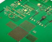
How to design a high speed pcb
Understanding Signal Integrity about how to design a high speed pcb
Designing a high-speed printed circuit board (PCB) necessitates a comprehensive understanding of signal integrity, which is paramount to ensuring the reliable performance of electronic systems.
Signal integrity refers to the quality and fidelity of electrical signals as they traverse the PCB, and it becomes increasingly critical as the speed of the signals rises. To achieve optimal signal integrity in high-speed PCB design, several key factors must be meticulously considered and addressed.
Firstly, the layout of the PCB plays a crucial role in maintaining signal integrity.
High-speed signals are susceptible to various forms of interference, such as crosstalk, electromagnetic interference (EMI), and signal reflections. To mitigate these issues, it is essential to carefully plan the placement of components and routing of traces. For instance, keeping high-speed signal traces as short and direct as possible can significantly reduce the potential for signal degradation. Additionally, maintaining adequate spacing between traces can help minimize crosstalk, which occurs when signals in adjacent traces interfere with each other.
Moreover, the choice of materials and stack-up configuration is another critical aspect of high-speed PCB design.
The dielectric material used in the PCB substrate can affect signal propagation speed and impedance. Selecting a material with a low dielectric constant and low loss tangent can enhance signal integrity by reducing signal attenuation and dispersion. Furthermore, a well-designed stack-up, which includes the arrangement of signal and power planes, can provide controlled impedance and effective shielding, thereby improving signal quality.
Transitioning to the topic of impedance control, it is imperative to ensure that the impedance of signal traces is consistent and matches the impedance of the connected components.
Impedance mismatches can lead to signal reflections, which can distort the signal and cause data errors. To achieve controlled impedance, designers must carefully calculate the trace width, spacing, and the distance between the trace and the reference plane. Utilizing simulation tools can aid in predicting and optimizing impedance values, thereby enhancing signal integrity.
In addition to impedance control, proper termination techniques are essential in high-speed PCB design.
Termination resistors can be used to match the impedance of the signal source and load, thereby minimizing reflections. There are various termination methods, such as series, parallel, and Thevenin termination, each with its own advantages and considerations. Selecting the appropriate termination method depends on the specific requirements of the design and the characteristics of the signals being transmitted.
Furthermore, power integrity is closely related to signal integrity and must not be overlooked.
High-speed circuits require stable and clean power delivery to function correctly. Power distribution networks (PDNs) should be designed to minimize noise and voltage fluctuations. This can be achieved by using decoupling capacitors strategically placed near power pins, employing multiple power and ground planes, and ensuring low impedance paths for current flow.
Lastly, grounding practices are vital for maintaining signal integrity in high-speed PCB design.
A solid ground plane can provide a low-impedance return path for signals, reducing the potential for ground bounce and EMI. Ensuring that all components have a reliable ground connection and avoiding ground loops can further enhance signal quality.
In conclusion, understanding and addressing signal integrity is fundamental to the successful design of high-speed PCBs. By carefully considering layout, material selection, impedance control, termination techniques, power integrity, and grounding practices, designers can mitigate potential issues and ensure the reliable performance of high-speed electronic systems. Employing these strategies will lead to robust and efficient PCB designs capable of meeting the demands of modern high-speed applications.

Best Practices for Layer Stackup in High-Speed PCB Design
Designing a high-speed printed circuit board (PCB) necessitates meticulous attention to detail, particularly in the layer stackup configuration. The layer stackup is a critical aspect that influences signal integrity, electromagnetic compatibility (EMC), and overall performance of the PCB. To achieve optimal results, it is essential to adhere to best practices that ensure the effective management of signal paths, power distribution, and thermal performance.
Firstly, it is imperative to understand the importance of layer arrangement.
A well-structured layer stackup minimizes signal interference and crosstalk, which are common issues in high-speed designs. Typically, a multi-layer PCB is preferred, as it allows for dedicated signal, power, and ground planes. By strategically placing these layers, designers can create a controlled impedance environment, which is crucial for maintaining signal integrity at high frequencies.
One of the fundamental principles in layer stackup design is the use of ground planes.
Ground planes serve as a reference for signal layers and help in reducing electromagnetic interference (EMI). Placing a ground plane adjacent to a signal layer creates a microstrip or stripline configuration, which is beneficial for controlling impedance. Moreover, it is advisable to have continuous ground planes without splits or gaps, as discontinuities can lead to signal reflections and degradation.
In addition to ground planes, power planes play a significant role in high-speed PCB design.
Power planes should be placed close to ground planes to form a low-inductance power distribution network. This proximity helps in decoupling high-frequency noise and provides a stable power supply to the components. Furthermore, using multiple power planes can enhance the current-carrying capacity and reduce voltage drops across the PCB.
Another best practice is to maintain symmetry in the layer stackup.
Symmetrical stackups help in balancing the mechanical stresses during the PCB manufacturing process, thereby reducing the risk of warping and bending. For instance, if a PCB has an eight-layer stackup, it is beneficial to have an equal number of signal and plane layers on both sides of the central core. This symmetry not only improves mechanical stability but also ensures uniform electrical performance.
Transitioning to the topic of signal routing, it is crucial to consider the trace width and spacing.
High-speed signals are susceptible to impedance mismatches, which can cause signal reflections and loss. Therefore, maintaining consistent trace width and spacing is essential for controlled impedance. Additionally, differential pairs, which are commonly used for high-speed data transmission, should be routed with equal lengths and minimal separation to preserve signal integrity.
Thermal management is another critical aspect of high-speed PCB design.
High-speed components often generate significant heat, which can affect performance and reliability. Incorporating thermal vias and heat sinks in the layer stackup can facilitate efficient heat dissipation. Moreover, using thicker copper layers for power and ground planes can enhance thermal conductivity and improve overall thermal performance.
In conclusion, designing a high-speed PCB requires a comprehensive understanding of layer stackup best practices. By carefully arranging signal, power, and ground layers, maintaining symmetry, and ensuring controlled impedance, designers can achieve superior signal integrity and EMC performance. Additionally, effective thermal management strategies are essential to ensure the reliability and longevity of the PCB. Adhering to these best practices will result in a high-speed PCB that meets the stringent demands of modern electronic applications.
Techniques for Minimizing Crosstalk in High-Speed PCB Layouts
Designing a high-speed printed circuit board (PCB) requires meticulous attention to detail, particularly when it comes to minimizing crosstalk. Crosstalk, the unwanted coupling of signals between adjacent traces, can significantly degrade the performance of high-speed circuits. To mitigate this issue, several techniques can be employed during the PCB layout process.
Firstly, maintaining adequate spacing between signal traces is crucial.
By increasing the distance between adjacent traces, the potential for electromagnetic interference is reduced. This is particularly important for high-speed signals, where even minor interference can lead to significant signal integrity issues. Utilizing differential pairs for high-speed signals can also be beneficial. Differential pairs consist of two traces carrying equal and opposite signals, which helps to cancel out any noise that may be induced in the traces.
In addition to spacing, the use of ground planes is another effective strategy.
Ground planes act as a reference point for signals and provide a low-impedance path for return currents. By placing a continuous ground plane adjacent to signal layers, the loop area for return currents is minimized, thereby reducing the potential for crosstalk. It is also advisable to ensure that the ground plane is as solid and uninterrupted as possible, avoiding any splits or gaps that could disrupt the return path.
Moreover, careful consideration of trace routing can further minimize crosstalk.
Routing high-speed signals on different layers, separated by ground planes, can significantly reduce the coupling between traces. When signals must cross each other, it is best to do so at right angles to minimize the interaction between the electromagnetic fields. Additionally, keeping high-speed signal traces as short as possible can help to reduce the potential for crosstalk, as longer traces are more susceptible to picking up unwanted signals.
Another technique involves the use of guard traces.
Guard traces are grounded traces placed between high-speed signal traces to provide additional shielding. These traces can absorb and redirect any coupled noise, thereby protecting the integrity of the signal. However, it is important to ensure that guard traces are properly grounded and do not introduce additional impedance mismatches.
Furthermore, the choice of materials and stack-up configuration plays a significant role in minimizing crosstalk.
High-quality dielectric materials with low loss tangents can help to maintain signal integrity by reducing signal attenuation and dispersion. A well-designed stack-up, with alternating signal and ground layers, can also provide effective isolation between high-speed signals and reduce the potential for crosstalk.
Lastly, implementing proper termination techniques is essential.
Impedance mismatches at the ends of signal traces can cause reflections, which can lead to crosstalk. By using appropriate termination resistors, the impedance of the trace can be matched to the source and load, thereby minimizing reflections and improving signal integrity.
In conclusion, minimizing crosstalk in high-speed PCB layouts requires a combination of techniques, including maintaining adequate spacing between traces, utilizing ground planes, careful trace routing, employing guard traces, selecting appropriate materials and stack-up configurations, and implementing proper termination techniques. By paying careful attention to these factors during the design process, the performance and reliability of high-speed PCBs can be significantly enhanced.
Importance of Controlled Impedance in High-Speed PCB Design
In the realm of high-speed PCB design, the importance of controlled impedance cannot be overstated. As electronic devices continue to evolve, the demand for faster data transmission rates and higher signal integrity has become paramount. Controlled impedance is a critical factor in ensuring that high-speed signals are transmitted with minimal distortion and loss, thereby maintaining the integrity of the data being communicated.
To begin with, controlled impedance refers to the characteristic impedance of a transmission line, which is determined by the physical dimensions and materials of the PCB traces and the surrounding dielectric. This impedance must be carefully managed to match the impedance of the source and load, thereby minimizing reflections and signal degradation. In high-speed circuits, even minor impedance mismatches can lead to significant signal integrity issues, such as ringing, crosstalk, and electromagnetic interference (EMI).
One of the primary reasons controlled impedance is crucial in high-speed PCB design is the need to maintain signal integrity.
High-speed signals, which often operate in the gigahertz range, are highly susceptible to distortion caused by impedance discontinuities. These discontinuities can occur at various points along the transmission path, such as vias, connectors, and component pads. By ensuring that the impedance is controlled and consistent throughout the PCB, designers can mitigate these issues and preserve the quality of the signal.
Moreover, controlled impedance is essential for minimizing signal reflections.
When a signal encounters an impedance mismatch, a portion of the signal is reflected back towards the source, causing interference with the original signal. This phenomenon, known as signal reflection, can lead to data corruption and communication errors. By designing transmission lines with controlled impedance, designers can ensure that the signal is transmitted efficiently, with minimal reflections and maximum fidelity.
In addition to signal integrity and reflection minimization, controlled impedance plays a vital role in reducing crosstalk. Crosstalk occurs when a signal in one transmission line induces an unwanted signal in an adjacent line, leading to interference and potential data errors. By maintaining controlled impedance, designers can reduce the coupling between adjacent traces, thereby minimizing crosstalk and enhancing overall signal quality.
Furthermore, controlled impedance is critical for managing electromagnetic interference (EMI).
High-speed signals can generate significant electromagnetic radiation, which can interfere with other electronic components and systems. By designing transmission lines with controlled impedance, designers can minimize the generation of EMI and ensure compliance with regulatory standards. This is particularly important in applications where electromagnetic compatibility (EMC) is a key consideration, such as in automotive, aerospace, and medical devices.
To achieve controlled impedance in high-speed PCB design, designers must carefully consider various factors, including trace width, trace spacing, dielectric material, and PCB stack-up. Advanced simulation tools and impedance calculators can aid in determining the optimal design parameters to achieve the desired impedance. Additionally, collaboration with PCB manufacturers is essential to ensure that the design specifications are accurately implemented during the fabrication process.
In conclusion, the importance of controlled impedance in high-speed PCB design cannot be underestimated. It is a fundamental aspect that directly impacts signal integrity, reflection minimization, crosstalk reduction, and EMI management. By meticulously designing transmission lines with controlled impedance, designers can ensure that high-speed signals are transmitted with minimal distortion and loss, thereby maintaining the integrity and reliability of the electronic system. As technology continues to advance, the need for controlled impedance in high-speed PCB design will only become more critical, underscoring its significance in the pursuit of optimal performance and functionality.