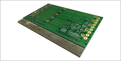
Multilayer pcb advantages
Enhanced Signal Integrity In Multilayer pcb advantages
Multilayer printed circuit boards (PCBs) have become a cornerstone in modern electronics, offering numerous advantages over their single-layer and double-layer counterparts.
One of the most significant benefits of multilayer PCBs is their enhanced signal integrity,
which is crucial for the performance and reliability of electronic devices.Signal integrity refers to the quality and reliability of electrical signals as they travel through the PCB, and it is a critical factor in high-speed and high-frequency applications.
To begin with, multilayer PCBs provide a more controlled environment for signal transmission.
By incorporating multiple layers, designers can allocate specific layers for signal routing, power distribution, and ground planes. This separation minimizes the interference between different signals, thereby reducing crosstalk and electromagnetic interference (EMI). Crosstalk occurs when a signal transmitted on one trace induces an unwanted signal on an adjacent trace, which can lead to data corruption and signal degradation. By strategically placing ground planes between signal layers, multilayer PCBs effectively shield signals from each other, enhancing overall signal integrity.
Furthermore, the use of ground planes in multilayer PCBs plays a pivotal role in maintaining signal integrity.
Ground planes act as a reference point for signals and provide a low-impedance path for return currents. This reduces the loop area of the signal path, thereby minimizing the inductance and potential for signal distortion. In high-speed circuits, where signal rise times are very short, even small inductances can cause significant signal integrity issues. The presence of continuous ground planes in multilayer PCBs helps to mitigate these problems, ensuring that signals remain clean and undistorted.
Another advantage of multilayer PCBs is their ability to support impedance control.
Impedance is the resistance to the flow of alternating current and is a critical parameter in high-frequency signal transmission. Variations in impedance can cause signal reflections, leading to data loss and communication errors. Multilayer PCBs allow for precise control of trace width, spacing, and dielectric thickness, enabling designers to achieve the desired impedance for specific signal traces. This level of control is challenging to achieve in single-layer or double-layer PCBs, making multilayer PCBs the preferred choice for high-speed and high-frequency applications.
Moreover, multilayer PCBs facilitate the implementation of differential signaling, a technique used to improve signal integrity in high-speed circuits.
Differential signaling involves transmitting two complementary signals on a pair of traces, with the difference between the signals representing the actual data. This method is highly effective in reducing noise and EMI, as any external interference affects both signals equally and is canceled out at the receiver. Multilayer PCBs provide the necessary layer structure to route differential pairs closely together, maintaining consistent impedance and minimizing signal skew.
In addition to these technical benefits, multilayer PCBs also contribute to the overall miniaturization and complexity of electronic devices.
By stacking multiple layers, designers can fit more circuitry into a smaller footprint, reducing the size and weight of the final product. This is particularly important in applications such as smartphones, medical devices, and aerospace electronics, where space and weight constraints are critical considerations.
In conclusion, the enhanced signal integrity offered by multilayer PCBs is a key factor driving their widespread adoption in modern electronics. The ability to control signal routing, minimize crosstalk and EMI, maintain consistent impedance, and support differential signaling makes multilayer PCBs an indispensable component in high-speed and high-frequency applications. As electronic devices continue to evolve and demand higher performance, the importance of multilayer PCBs in ensuring reliable and efficient signal transmission will only continue to grow.
Space And Weight Reduction With Multilayer PCBs
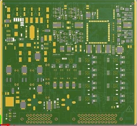
Multilayer printed circuit boards (PCBs) have become a cornerstone in modern electronics, offering numerous advantages over their single-layer and double-layer counterparts.
One of the most significant benefits of multilayer PCBs is their ability to reduce both space and weight in electronic devices,
which is crucial in today’s technology-driven world. As electronic devices continue to shrink in size while increasing in functionality, the demand for compact and lightweight components has never been higher. Multilayer PCBs address this need effectively, providing a solution that enhances performance without compromising on space or weight.
To begin with, multilayer PCBs consist of multiple layers of conductive material separated by insulating layers,
all laminated together into a single, compact board. This design allows for a higher density of components and interconnections within a smaller footprint. By stacking multiple layers, designers can incorporate more complex circuits into a limited space, which is particularly beneficial for devices where size constraints are critical, such as smartphones, tablets, and wearable technology. The ability to integrate more functionality into a smaller area not only saves space but also contributes to the overall miniaturization of electronic devices.
Moreover, the reduction in space directly correlates with a reduction in weight.
Multilayer PCBs eliminate the need for multiple single-layer boards and the associated interconnecting wires and connectors, which can add significant bulk and weight to a device. By consolidating the circuitry into a single multilayer board, the overall weight of the electronic device is significantly reduced. This is especially advantageous in applications where weight is a critical factor, such as in aerospace, automotive, and medical devices. For instance, in aerospace applications, every gram saved can contribute to fuel efficiency and overall performance, making multilayer PCBs an ideal choice.
In addition to space and weight reduction, multilayer PCBs offer improved electrical performance.
The close proximity of the layers allows for shorter signal paths, which reduces signal loss and improves signal integrity. This is particularly important in high-speed and high-frequency applications where maintaining signal quality is paramount. The enhanced electrical performance of multilayer PCBs not only contributes to the overall efficiency of the device but also enables the integration of more advanced features and functionalities.
Furthermore, the use of multilayer PCBs can lead to cost savings in the long run.
Although the initial manufacturing cost of multilayer PCBs may be higher compared to single-layer or double-layer boards, the benefits of reduced space and weight, along with improved performance, can result in lower overall system costs. For example, the compact design can lead to smaller enclosures and housings, which can reduce material costs. Additionally, the improved reliability and performance can lead to fewer failures and lower maintenance costs over the device’s lifespan.
In conclusion, the advantages of multilayer PCBs in terms of space and weight reduction are clear. By enabling the integration of more complex circuits into a smaller and lighter package, multilayer PCBs play a crucial role in the advancement of modern electronic devices. Their ability to enhance electrical performance and contribute to cost savings further solidifies their importance in various high-tech applications. As technology continues to evolve, the demand for compact, lightweight, and high-performance components will only increase, making multilayer PCBs an indispensable element in the design and development of future electronic devices.
Improved Design Flexibility In Multilayer PCBs
Multilayer printed circuit boards (PCBs) have revolutionized the electronics industry by offering enhanced design flexibility, which is crucial for the development of complex and high-performance electronic devices. This flexibility stems from the ability to incorporate multiple layers of circuitry within a single board, allowing for more intricate and compact designs. As a result, multilayer PCBs have become indispensable in various applications, ranging from consumer electronics to advanced aerospace systems.
One of the primary advantages of multilayer PCBs is their capacity to support higher component density.
By stacking multiple layers of circuits, designers can integrate a greater number of components within a limited space. This is particularly beneficial for modern electronic devices, which demand miniaturization without compromising functionality. For instance, smartphones, tablets, and wearable devices all rely on multilayer PCBs to achieve their sleek and compact form factors while maintaining robust performance.
Moreover, the improved design flexibility of multilayer PCBs facilitates the implementation of more complex circuitry.
With single-layer or double-layer PCBs, designers often face constraints in routing traces and managing signal integrity. However, multilayer PCBs provide additional routing layers, which can be used to separate different signal paths and reduce electromagnetic interference (EMI). This separation is critical for high-speed digital circuits, where signal integrity is paramount. Consequently, multilayer PCBs enable the development of high-frequency and high-speed applications, such as advanced communication systems and high-performance computing devices.
In addition to supporting higher component density and complex circuitry, multilayer PCBs also offer enhanced thermal management capabilities.
The multiple layers can be designed to include dedicated ground and power planes, which help dissipate heat more effectively. This is particularly important for power-intensive applications, where efficient thermal management is essential to ensure reliable operation and prevent overheating. By incorporating thermal vias and strategically placing heat-dissipating components, multilayer PCBs can maintain optimal operating temperatures, thereby extending the lifespan of electronic devices.
Furthermore, the design flexibility of multilayer PCBs allows for the integration of various functionalities within a single board.
This integration reduces the need for multiple interconnected PCBs, which can simplify the overall design and assembly process. For example, in automotive electronics, multilayer PCBs can combine control, communication, and power management functions into a single board, resulting in a more compact and reliable system. This consolidation not only enhances performance but also reduces manufacturing costs and improves product reliability.
Another significant advantage of multilayer PCBs is their ability to support advanced manufacturing techniques.
The use of sophisticated fabrication processes, such as laser drilling and sequential lamination, enables the production of high-precision and high-quality multilayer boards. These advanced techniques allow for tighter tolerances and finer pitch components, which are essential for modern electronic devices. Consequently, multilayer PCBs can meet the stringent requirements of cutting-edge applications, such as medical devices and aerospace systems, where precision and reliability are critical.
In conclusion, the improved design flexibility of multilayer PCBs offers numerous advantages that are essential for the development of modern electronic devices. By supporting higher component density, enabling complex circuitry, enhancing thermal management, integrating multiple functionalities, and accommodating advanced manufacturing techniques, multilayer PCBs have become a cornerstone of the electronics industry. As technology continues to evolve, the demand for multilayer PCBs is expected to grow, further driving innovation and enabling the creation of more sophisticated and high-performance electronic systems.
Increased Durability And Reliability Of Multilayer PCBs
Multilayer printed circuit boards (PCBs) have become a cornerstone in modern electronics, offering numerous advantages over their single-layer and double-layer counterparts. One of the most significant benefits of multilayer PCBs is their increased durability and reliability, which are critical factors in the performance and longevity of electronic devices. This article delves into the reasons behind the enhanced durability and reliability of multilayer PCBs, providing a comprehensive understanding of their superiority in these aspects.
To begin with, the structural integrity of multilayer PCBs is inherently superior due to their complex construction.
These PCBs consist of multiple layers of conductive material, typically copper, separated by insulating layers. This layered configuration not only allows for a higher density of components and connections but also contributes to the overall robustness of the board. The multiple layers are laminated together under high pressure and temperature, creating a solid and unified structure that is less prone to mechanical stress and damage. Consequently, multilayer PCBs can withstand harsher environmental conditions and physical impacts, making them ideal for applications in demanding industries such as aerospace, automotive, and industrial machinery.
Moreover, the reliability of multilayer PCBs is significantly enhanced by their ability to reduce electromagnetic interference (EMI).
In electronic circuits, EMI can cause signal degradation and data loss, leading to malfunctions and reduced performance. Multilayer PCBs mitigate this issue by incorporating ground and power planes within their layers. These planes act as shields, isolating sensitive signal traces from potential sources of interference. By minimizing EMI, multilayer PCBs ensure more stable and reliable operation of electronic devices, which is particularly crucial in high-frequency applications and communication systems.
Another factor contributing to the increased reliability of multilayer PCBs is their improved thermal management capabilities.
Electronic components generate heat during operation, and excessive heat can lead to component failure and reduced lifespan of the device. Multilayer PCBs are designed to efficiently dissipate heat through their multiple layers, which can include dedicated thermal vias and heat sinks. This effective thermal management prevents overheating and ensures that components operate within their optimal temperature range, thereby enhancing the overall reliability of the device.
Furthermore, the advanced manufacturing processes used in the production of multilayer PCBs contribute to their durability and reliability.
These processes involve precise fabrication techniques, such as laser drilling and advanced plating methods, which result in high-quality and defect-free boards. The use of high-grade materials, including specialized laminates and solder masks, also plays a crucial role in ensuring the longevity and performance of multilayer PCBs. These materials are selected for their excellent electrical, thermal, and mechanical properties, which further enhance the durability and reliability of the final product.
In addition to these technical advantages, the design flexibility offered by multilayer PCBs allows for the incorporation of redundant pathways and backup systems.
This redundancy ensures that even if one pathway fails, the circuit can continue to function through an alternative route, thereby increasing the overall reliability of the device. This feature is particularly valuable in mission-critical applications where system failure is not an option.
In conclusion, the increased durability and reliability of multilayer PCBs stem from their robust construction, effective EMI reduction, superior thermal management, advanced manufacturing processes, and design flexibility. These attributes make multilayer PCBs an indispensable component in modern electronics, ensuring the optimal performance and longevity of devices across various industries. As technology continues to advance, the demand for durable and reliable multilayer PCBs is expected to grow, further solidifying their importance in the ever-evolving landscape of electronic design and manufacturing.