Multilayer pcb fabrication process
Introduction To Multilayer PCB Fabrication
The fabrication of multilayer printed circuit boards (PCBs) is a sophisticated process that involves several intricate steps, each crucial to the final product’s performance and reliability.
Multilayer PCBs, which consist of multiple layers of conductive material separated by insulating layers, are essential in modern electronics due to their ability to support complex circuitry in a compact form. Understanding the fabrication process of these advanced PCBs is fundamental for anyone involved in electronics design and manufacturing.
To begin with, the process starts with the design phase, where engineers use specialized software to create a detailed layout of the PCB.
This layout includes the placement of components, the routing of electrical connections, and the definition of the various layers. Once the design is finalized, it is converted into a format suitable for manufacturing, typically Gerber files, which contain all the necessary information for each layer of the PCB.
Following the design phase, the actual fabrication process commences with the preparation of the base materials.
The core of a multilayer PCB is usually made of a fiberglass-reinforced epoxy laminate, known as FR4. This material provides the necessary mechanical strength and electrical insulation. Copper foil is then laminated onto both sides of the FR4 core, forming the initial conductive layers. For multilayer PCBs, additional layers of copper and insulating material are added in a sequential manner.
The next step involves the creation of the inner layers.
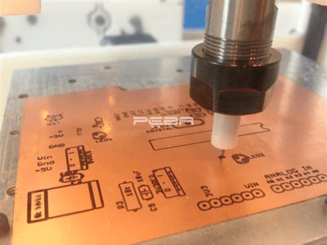
Each inner layer is printed with the circuit pattern using a photolithographic process. A photosensitive film, or photoresist, is applied to the copper surface, and the circuit pattern is transferred onto the film using ultraviolet light. The exposed areas of the photoresist are then developed, revealing the underlying copper, which is subsequently etched away to form the desired circuit pattern. This process is repeated for each inner layer, ensuring precise alignment and accuracy.
Once the inner layers are completed, they are stacked together with layers of insulating material, typically pre-preg, which is a fiberglass cloth impregnated with resin.
The stack is then subjected to heat and pressure in a process called lamination, which bonds the layers together into a single, solid structure. This laminated structure is then drilled to create holes for the electrical connections between the layers, known as vias. The drilling process must be highly accurate to ensure proper alignment and connectivity.
After drilling, the holes are plated with copper to establish electrical connections between the layers.
This is achieved through an electroplating process, where the entire board is submerged in a copper plating solution, and an electric current is applied to deposit copper onto the exposed surfaces, including the walls of the drilled holes. This step is critical for ensuring reliable electrical performance.
The outer layers of the PCB are then processed in a similar manner to the inner layers, with the circuit pattern being transferred using photolithography and etching.
Once the outer layers are completed, the board undergoes a series of finishing processes, including solder mask application, surface finish plating, and silkscreen printing. The solder mask is a protective layer that prevents solder from bridging between conductive traces, while the surface finish plating, such as gold or silver, enhances solderability and protects the copper from oxidation. The silkscreen printing adds component labels and other markings to the board.
Finally, the completed PCB is subjected to rigorous testing to ensure it meets all design specifications and quality standards.
This includes electrical testing to verify connectivity and functionality, as well as visual inspections to check for any defects or imperfections. Once the PCB passes all tests, it is ready for assembly and integration into electronic devices.
In conclusion, the fabrication of multilayer PCBs is a complex and precise process that requires careful attention to detail at every step. From design and material preparation to layer processing and final testing, each stage plays a vital role in producing high-quality PCBs that meet the demands of modern electronics.
Key Steps In Multilayer PCB Manufacturing
The multilayer PCB fabrication process is a sophisticated and intricate procedure that involves several key steps to ensure the production of high-quality printed circuit boards. This process begins with the design phase, where engineers use specialized software to create a detailed blueprint of the PCB. This blueprint includes the layout of the various layers, the placement of components, and the routing of electrical connections. Once the design is finalized, it is converted into a format that can be used by the fabrication equipment.
Following the design phase, the next step is the preparation of the materials.
This involves selecting the appropriate substrate, typically a fiberglass-reinforced epoxy laminate, and cutting it to the required dimensions. The substrate serves as the foundation for the PCB and provides mechanical support and electrical insulation. In addition to the substrate, copper foil is also prepared, which will be used to form the conductive layers of the PCB.
The process then moves on to the creation of the inner layers.
Each inner layer is produced by laminating a sheet of copper foil onto the substrate and then applying a photoresist material. The photoresist is a light-sensitive coating that allows for the precise transfer of the circuit design onto the copper foil. The circuit design is then printed onto the photoresist using a photolithographic process, which involves exposing the photoresist to ultraviolet light through a photomask. The exposed areas of the photoresist harden, while the unexposed areas remain soft and can be washed away, revealing the underlying copper.
Once the photoresist has been developed, the next step is etching.
During etching, the exposed copper is removed using a chemical solution, leaving behind the desired circuit pattern. After etching, the remaining photoresist is stripped away, and the inner layers are inspected for any defects. If any issues are found, they are corrected before proceeding to the next step.
The inner layers are then laminated together to form a single multilayer structure.
This is achieved by stacking the layers in the correct order and bonding them together using heat and pressure. The lamination process also includes the addition of prepreg, a partially cured epoxy resin, which helps to bond the layers together and provides additional insulation. The laminated structure is then drilled to create holes for the electrical connections between the layers and for mounting components.
After drilling, the holes are plated with copper to establish electrical connections between the layers.
This is followed by the application of a solder mask, which is a protective coating that prevents solder from bridging between conductive areas during the assembly process. The solder mask is applied using a similar photolithographic process as the one used for the inner layers.
The final steps in the multilayer PCB fabrication process include the application of a surface finish, which protects the exposed copper and enhances solderability, and the addition of silkscreen markings, which provide information about the PCB and its components. The completed PCB is then subjected to rigorous testing to ensure that it meets all design specifications and performance requirements.
In conclusion, the multilayer PCB fabrication process is a complex and precise procedure that involves multiple steps, each of which is critical to the production of high-quality printed circuit boards. From design and material preparation to lamination, drilling, and finishing, each stage must be carefully executed to ensure the reliability and functionality of the final product.
Challenges In Multilayer PCB Production
The fabrication of multilayer printed circuit boards (PCBs) is a complex and intricate process that presents numerous challenges. These challenges stem from the need to ensure precision, reliability, and functionality in increasingly compact and sophisticated electronic devices. One of the primary difficulties in multilayer PCB production is the alignment of the various layers. Each layer must be meticulously aligned to ensure that the electrical connections between them are accurate. Misalignment can lead to short circuits, open circuits, or other defects that compromise the performance of the final product. This requires advanced machinery and highly skilled technicians to achieve the necessary precision.
Another significant challenge is the management of thermal expansion.
Different materials used in the construction of PCBs, such as copper and various substrates, expand and contract at different rates when exposed to temperature changes. This can cause warping or delamination of the layers, leading to potential failure of the PCB. To mitigate this, manufacturers must carefully select materials with compatible thermal expansion coefficients and employ precise temperature control during the fabrication process.
The drilling process also poses a challenge in multilayer PCB production.
Vias, or small holes, must be drilled through the layers to create electrical connections between them. The drilling must be precise to avoid damaging the surrounding material and to ensure that the vias are properly plated with conductive material. This requires advanced drilling equipment and techniques, such as laser drilling, to achieve the necessary accuracy and consistency.
Furthermore, the etching process, which involves removing unwanted copper to create the desired circuit patterns, must be carefully controlled.
Over-etching can remove too much material, while under-etching can leave excess copper, both of which can lead to circuit failures. The etching process must be precisely timed and monitored to ensure that the correct amount of material is removed.
The lamination process, where the individual layers are bonded together under heat and pressure, also presents challenges. Any impurities or air bubbles trapped between the layers can cause delamination or other defects. The lamination process must be conducted in a clean environment, and the pressure and temperature must be carefully controlled to ensure a strong and uniform bond between the layers.
In addition to these technical challenges, there are also logistical and economic considerations.
The production of multilayer PCBs requires significant investment in advanced machinery and skilled labor. The cost of materials, particularly high-quality substrates and copper, can also be substantial. Manufacturers must balance the need for precision and quality with the constraints of budget and production timelines.
Moreover, as electronic devices continue to evolve, the demand for more complex and higher-density PCBs increases.
This drives the need for continuous innovation and improvement in fabrication techniques. Manufacturers must stay abreast of the latest technological advancements and continuously refine their processes to meet the ever-growing demands of the industry.
In conclusion, the production of multilayer PCBs is fraught with challenges that require a combination of advanced technology, skilled labor, and meticulous attention to detail. From alignment and thermal management to drilling, etching, and lamination, each step of the process must be carefully controlled to ensure the reliability and functionality of the final product. As the demand for more sophisticated electronic devices continues to rise, manufacturers must continually innovate and improve their techniques to overcome these challenges and deliver high-quality PCBs.
Quality Control In Multilayer PCB Fabrication
Quality control in multilayer PCB fabrication is a critical aspect that ensures the reliability and performance of the final product. The process begins with the meticulous selection of raw materials, as the quality of the base materials directly impacts the overall integrity of the PCB. High-grade copper-clad laminates and prepregs are chosen to provide a stable foundation for the multilayer structure. Once the materials are selected, they undergo rigorous inspection to detect any defects or inconsistencies that could compromise the PCB’s functionality.
Following the material inspection, the fabrication process moves to the inner layer imaging stage.
Here, photoresist is applied to the copper-clad laminates, and a photolithographic process is used to transfer the circuit pattern onto the laminate. This step requires precise alignment and exposure to ensure that the circuit patterns are accurately replicated. Any deviation in this stage can lead to misalignment in the subsequent layers, which can cause electrical failures. Therefore, quality control measures such as automated optical inspection (AOI) are employed to verify the accuracy of the circuit patterns before proceeding to the next step.
The next phase involves the etching process, where unwanted copper is removed to reveal the desired circuit traces.
This step is followed by a thorough cleaning to remove any residual chemicals that could affect the adhesion of subsequent layers. Quality control at this stage includes checking for under-etching or over-etching, which can lead to circuit shorts or opens. Advanced inspection techniques, such as X-ray fluorescence (XRF), are used to measure the thickness of the copper traces and ensure they meet the specified requirements.
Once the inner layers are prepared, they are laminated together under high pressure and temperature to form a single multilayer board.
This lamination process is critical, as any misalignment or air entrapment can lead to delamination or voids, which can severely impact the PCB’s performance. Quality control during lamination involves using X-ray inspection to detect any internal defects and ensure proper alignment of the layers.
After lamination, the outer layers are imaged and etched in a similar manner to the inner layers.
This is followed by drilling, where holes are created for vias and through-hole components. The precision of the drilling process is crucial, as any deviation can affect the electrical connectivity and mechanical stability of the PCB. Quality control measures include using automated drilling machines with high precision and conducting post-drilling inspections to verify the accuracy of the hole placement and size.
The final stages of the fabrication process involve plating, solder mask application, and surface finish.
Plating ensures that the vias and through-holes are electrically conductive, while the solder mask protects the circuit traces from oxidation and prevents solder bridges during component assembly. The surface finish, such as HASL, ENIG, or OSP, provides a solderable surface for component attachment. Quality control in these stages includes inspecting the plating thickness, solder mask alignment, and surface finish uniformity to ensure they meet the required specifications.
In conclusion, quality control in multilayer PCB fabrication is a comprehensive process that encompasses every stage of production, from material selection to final inspection. By implementing stringent quality control measures, manufacturers can ensure that the final product meets the highest standards of reliability and performance, ultimately leading to the successful deployment of electronic devices in various applications.