Multilayer pcb stackup
Importance Of Multilayer PCB Stackup In Modern Electronics
In the realm of modern electronics, the importance of multilayer PCB stackup cannot be overstated. As electronic devices become increasingly complex and compact, the demand for efficient and reliable printed circuit boards (PCBs) has surged. Multilayer PCBs, which consist of multiple layers of conductive material separated by insulating layers, have emerged as a critical solution to meet these demands. The stackup of these layers plays a pivotal role in determining the performance, reliability, and manufacturability of the final product.
One of the primary reasons multilayer PCB stackup is so crucial is its impact on signal integrity.
In high-speed electronic circuits, signal integrity is paramount to ensure that data is transmitted accurately and without distortion. The arrangement of layers in a multilayer PCB stackup can significantly influence the impedance of signal traces, which in turn affects signal quality. By carefully designing the stackup, engineers can control the impedance and minimize signal loss, crosstalk, and electromagnetic interference (EMI). This is particularly important in applications such as telecommunications, computing, and automotive electronics, where high-speed data transmission is essential.
Moreover, the multilayer PCB stackup is instrumental in enhancing the thermal management of electronic devices.
As electronic components become more powerful, they generate more heat, which must be efficiently dissipated to prevent overheating and ensure reliable operation. The stackup design can incorporate thermal vias and dedicated heat dissipation layers to facilitate the transfer of heat away from critical components. This is especially vital in applications like power electronics and LED lighting, where thermal performance directly impacts the longevity and efficiency of the device.
In addition to signal integrity and thermal management, the multilayer PCB stackup also plays a key role in reducing the overall size and weight of electronic devices.
By integrating multiple layers into a single PCB, designers can achieve higher component density and more complex routing, which allows for more compact and lightweight designs. This is particularly advantageous in portable and wearable electronics, where space and weight constraints are critical considerations. Furthermore, the ability to incorporate multiple functions into a single PCB reduces the need for additional interconnections and components, leading to cost savings and improved reliability.
Transitioning to the manufacturability aspect, the multilayer PCB stackup is essential for ensuring that the PCB can be produced efficiently and with high yield.
The stackup design must take into account factors such as layer alignment, drilling precision, and material selection to ensure that the PCB can be fabricated without defects. Additionally, the stackup must be compatible with the chosen manufacturing processes, such as lamination and etching, to achieve the desired performance characteristics. By optimizing the stackup design, manufacturers can achieve higher production yields and lower costs, which is crucial in the competitive electronics market.
Furthermore, the multilayer PCB stackup is a critical consideration in the context of electromagnetic compatibility (EMC).
As electronic devices operate at higher frequencies and power levels, they are more susceptible to EMI, which can cause malfunctions and degrade performance. The stackup design can incorporate shielding layers and ground planes to mitigate EMI and ensure compliance with EMC regulations. This is particularly important in industries such as aerospace and medical devices, where stringent EMC standards must be met to ensure safety and reliability.
In conclusion, the importance of multilayer PCB stackup in modern electronics is multifaceted, encompassing signal integrity, thermal management, size and weight reduction, manufacturability, and electromagnetic compatibility. As electronic devices continue to evolve and become more sophisticated, the role of multilayer PCB stackup in achieving optimal performance and reliability will only become more critical. By carefully designing and optimizing the stackup, engineers can meet the ever-increasing demands of modern electronics and pave the way for future innovations.
Key Considerations For Designing A Multilayer PCB Stackup
Designing a multilayer PCB stackup is a complex process that requires careful consideration of various factors to ensure optimal performance and reliability. One of the primary considerations is the selection of materials. The choice of dielectric materials and copper foils significantly impacts the electrical performance, thermal management, and mechanical stability of the PCB. High-frequency applications, for instance, demand materials with low dielectric constants and low loss tangents to minimize signal degradation. Additionally, the thermal properties of the materials must be compatible with the operating environment to prevent overheating and ensure longevity.
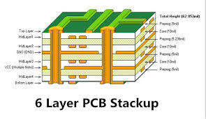
Another critical aspect is the layer configuration.
The arrangement of signal, power, and ground layers within the stackup influences the electromagnetic compatibility (EMC) and signal integrity of the PCB. A well-designed stackup typically alternates signal layers with ground or power planes to provide effective shielding and reduce electromagnetic interference (EMI). This configuration also helps in maintaining controlled impedance, which is crucial for high-speed signal transmission. Furthermore, the symmetry of the stackup should be maintained to prevent warping during the manufacturing process, which can lead to mechanical failures.
The thickness of each layer is also a vital consideration.
The overall thickness of the PCB affects its flexibility, thermal performance, and the ability to accommodate through-hole components. Thinner layers can improve signal integrity by reducing the distance between signal and reference planes, thereby minimizing crosstalk and signal loss. However, they may also increase the risk of mechanical damage and complicate the manufacturing process. Therefore, a balance must be struck between electrical performance and mechanical robustness.
Via design is another important factor in multilayer PCB stackup.
Vias are used to establish electrical connections between different layers, and their placement and size can significantly impact the board’s performance. Blind and buried vias, which connect only specific layers, can help in reducing the complexity of the routing and improving signal integrity. However, they also increase the manufacturing cost and complexity. The aspect ratio of the vias, which is the ratio of the hole depth to its diameter, should be optimized to ensure reliable plating and avoid potential failures.
Thermal management is a crucial consideration, especially for high-power applications.
The stackup design should facilitate efficient heat dissipation to prevent overheating and ensure reliable operation. This can be achieved by incorporating thermal vias, using materials with high thermal conductivity, and optimizing the placement of heat-generating components. Additionally, the stackup should be designed to accommodate thermal expansion and contraction to prevent mechanical stress and potential failures.
Manufacturability is another key consideration in multilayer PCB stackup design.
The complexity of the stackup should be balanced with the capabilities of the manufacturing process to ensure cost-effectiveness and high yield. Design for manufacturability (DFM) principles should be applied to minimize potential issues during production, such as misalignment, delamination, and insufficient plating. Collaboration with the PCB manufacturer during the design phase can help in identifying potential challenges and optimizing the stackup for efficient production.
In conclusion, designing a multilayer PCB stackup involves a careful balance of material selection, layer configuration, thickness optimization, via design, thermal management, and manufacturability. Each of these factors plays a crucial role in determining the electrical performance, mechanical stability, and overall reliability of the PCB. By considering these key aspects and applying best practices, designers can create robust and efficient multilayer PCBs that meet the demands of modern electronic applications.
Common Mistakes To Avoid In Multilayer PCB Stackup Design
Designing a multilayer PCB stackup is a complex process that requires meticulous attention to detail. One common mistake is neglecting to properly plan the layer arrangement. The sequence of layers in a PCB stackup significantly impacts signal integrity, thermal management, and overall performance. Designers often overlook the importance of placing power and ground planes strategically. These planes should be adjacent to signal layers to provide effective return paths and minimize electromagnetic interference (EMI). Failing to do so can result in increased noise and signal degradation.
Another frequent error is inadequate consideration of impedance control.
Impedance mismatches can lead to signal reflections, which degrade signal quality and can cause data errors. To avoid this, designers must carefully calculate and control the impedance of signal traces, especially in high-speed circuits. This involves selecting appropriate materials, adjusting trace widths, and maintaining consistent spacing between traces and planes. Ignoring these factors can compromise the reliability and performance of the PCB.
Thermal management is another critical aspect that is often underestimated
Multilayer PCBs can generate significant heat, especially in high-power applications. Designers must ensure that heat is effectively dissipated to prevent overheating and potential damage to components. This can be achieved by incorporating thermal vias, using materials with high thermal conductivity, and optimizing the placement of heat-generating components. Neglecting thermal management can lead to reduced lifespan and reliability of the PCB.
Furthermore, designers sometimes fail to account for manufacturing tolerances.
Variations in material properties, etching processes, and layer alignment can affect the final dimensions and performance of the PCB. It is essential to work closely with the manufacturer to understand their capabilities and limitations. This includes specifying acceptable tolerances and conducting thorough design reviews to identify potential issues early in the design process. Overlooking these factors can result in costly rework and delays in production.
Additionally, insufficient attention to signal integrity can lead to various issues.
Crosstalk, for instance, occurs when signals on adjacent traces interfere with each other. This can be mitigated by maintaining adequate spacing between traces, using differential pairs for high-speed signals, and incorporating ground planes to shield sensitive signals. Another aspect of signal integrity is the management of signal return paths. Ensuring that return paths are short and direct helps minimize loop areas and reduces the risk of EMI.
Moreover, designers often underestimate the importance of proper documentation.
Comprehensive documentation, including detailed layer stackup diagrams, material specifications, and design rules, is crucial for successful PCB fabrication and assembly. Incomplete or inaccurate documentation can lead to misunderstandings and errors during manufacturing, resulting in defective PCBs.
Lastly, it is essential to consider the overall design for manufacturability (DFM).
This involves designing the PCB in a way that facilitates efficient and cost-effective manufacturing. Factors such as panelization, component placement, and routing should be optimized to minimize production costs and improve yield. Ignoring DFM principles can lead to increased production costs and lower quality PCBs.
In conclusion, avoiding common mistakes in multilayer PCB stackup design requires careful planning, attention to detail, and collaboration with manufacturers. By addressing issues such as layer arrangement, impedance control, thermal management, manufacturing tolerances, signal integrity, documentation, and DFM, designers can ensure the reliability and performance of their PCBs.
Advanced Techniques For Optimizing Multilayer PCB Stackup
Optimizing multilayer PCB stackup is a critical aspect of modern electronics design, as it directly influences the performance, reliability, and manufacturability of the final product. Advanced techniques in this domain are essential for engineers aiming to meet the stringent demands of high-speed, high-density applications. One of the primary considerations in multilayer PCB stackup is the arrangement of signal, power, and ground layers. Proper layer arrangement minimizes electromagnetic interference (EMI) and crosstalk, which are detrimental to signal integrity. By strategically placing ground planes adjacent to signal layers, designers can create controlled impedance environments that enhance signal quality and reduce noise.
Another advanced technique involves the use of differential pairs for high-speed signal transmission.
Differential pairs consist of two traces carrying equal and opposite signals, which helps to cancel out noise and improve signal integrity. Ensuring that these pairs are routed symmetrically and maintaining consistent spacing between them is crucial. This practice minimizes skew and ensures that the signals arrive at their destination simultaneously, which is vital for maintaining data integrity in high-speed applications.
Thermal management is another critical aspect of multilayer PCB stackup optimization.
As electronic devices become more powerful, they generate more heat, which can affect performance and longevity. Advanced techniques such as incorporating thermal vias and using materials with high thermal conductivity can help dissipate heat more effectively. Thermal vias are small holes filled with conductive material that connect different layers of the PCB, allowing heat to transfer from hot components to cooler areas or to a heat sink.
Furthermore, the choice of materials plays a significant role in optimizing multilayer PCB stackup.
High-frequency applications, for instance, require materials with low dielectric constant and low loss tangent to minimize signal attenuation and distortion. Advanced materials such as PTFE (polytetrafluoroethylene) and ceramic-filled laminates are often used in these scenarios. Additionally, selecting materials with similar coefficients of thermal expansion (CTE) can prevent mechanical stress and potential failure due to temperature variations.
Signal integrity can also be enhanced through the use of advanced simulation tools.
These tools allow designers to model and analyze the electrical behavior of their PCB stackup before physical prototyping. By simulating different stackup configurations, trace widths, and spacing, engineers can identify potential issues and optimize their designs for better performance. This approach not only saves time and resources but also leads to more reliable and efficient PCBs.
Moreover, the integration of blind and buried vias is an advanced technique that can significantly improve multilayer PCB stackup.
Blind vias connect an outer layer to one or more inner layers without passing through the entire board, while buried vias connect inner layers without reaching the outer layers. These vias help to reduce the number of through-hole vias, which can occupy valuable real estate on the PCB and complicate routing. By using blind and buried vias, designers can achieve higher density and more efficient routing, which is particularly beneficial for complex, high-speed designs.
In conclusion, optimizing multilayer PCB stackup requires a comprehensive understanding of various advanced techniques and their implications on signal integrity, thermal management, and manufacturability. By carefully considering layer arrangement, differential pair routing, thermal management strategies, material selection, simulation tools, and via integration, engineers can design PCBs that meet the demanding requirements of modern electronic applications. These advanced techniques not only enhance the performance and reliability of the final product but also contribute to more efficient and cost-effective manufacturing processes.