Resistance of pcb trace high frequency
Understanding The Impact Of Resistance of pcb trace high frequency
Understanding the impact of high frequency on PCB trace resistance is crucial for the design and performance of modern electronic circuits. As electronic devices continue to evolve, operating at higher frequencies has become a necessity to meet the demands for faster data transmission and more efficient performance. However, this shift towards higher frequencies introduces several challenges, one of which is the increased resistance of PCB traces.
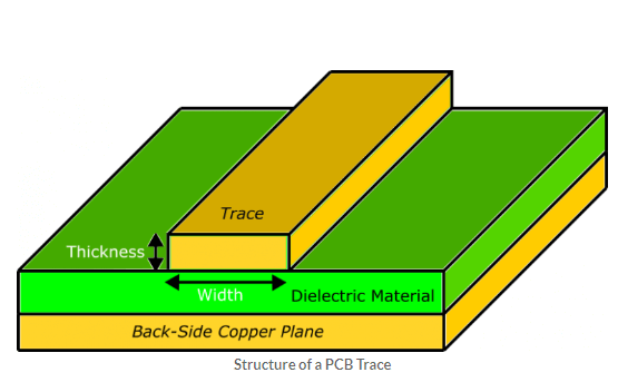
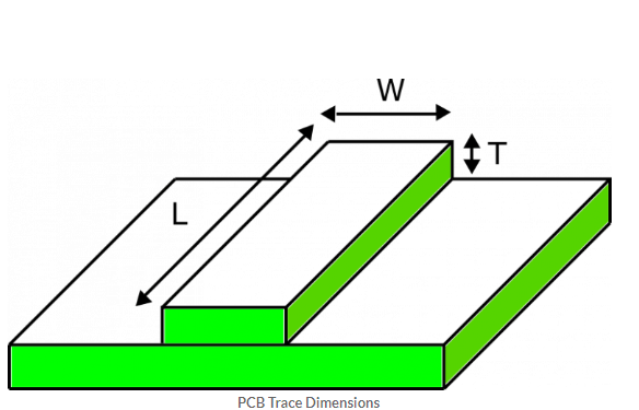
At low frequencies, the resistance of a PCB trace is primarily determined by its material properties, length, and cross-sectional area. Copper, commonly used for PCB traces, exhibits low resistivity, making it an ideal conductor for most applications. However, as the frequency of the signal increases, additional factors come into play, significantly affecting the trace resistance.
One of the primary phenomena that contribute to increased resistance at high frequencies is the skin effect.
The skin effect causes the alternating current (AC) to concentrate near the surface of the conductor, effectively reducing the cross-sectional area through which the current flows. This reduction in effective area leads to an increase in the trace resistance. The skin depth, which is the depth at which the current density falls to 1/e (about 37%) of its value at the surface, decreases with increasing frequency. Consequently, at very high frequencies, the current is confined to an extremely thin layer on the surface of the trace, exacerbating the resistance.
In addition to the skin effect, the proximity effect also plays a significant role in increasing PCB trace resistance at high frequencies.
The proximity effect occurs when multiple conductors carrying AC signals are placed close to each other. The magnetic fields generated by the currents in these conductors interact, causing the current to redistribute within each conductor. This redistribution results in higher current density in certain regions, further increasing the resistance. The proximity effect is particularly pronounced in densely packed PCBs where traces are in close proximity.
Moreover, the dielectric properties of the PCB material can influence the resistance of traces at high frequencies.
The dielectric constant and loss tangent of the substrate material affect the propagation of high-frequency signals. Materials with higher dielectric constants can cause signal attenuation and dispersion, leading to increased effective resistance. Therefore, selecting appropriate PCB materials with low dielectric losses is essential for minimizing resistance at high frequencies.
To mitigate the impact of high frequency on PCB trace resistance, several design strategies can be employed.
One approach is to use wider traces, which can help reduce the resistance by providing a larger cross-sectional area for current flow. However, this solution may not always be feasible due to space constraints on the PCB. Another strategy is to use multiple layers of traces connected in parallel, effectively increasing the overall cross-sectional area and reducing resistance. Additionally, employing high-frequency laminates with low dielectric losses can help maintain signal integrity and minimize resistance.
In conclusion, understanding the impact of high frequency on PCB trace resistance is vital for designing efficient and reliable electronic circuits. The skin effect, proximity effect, and dielectric properties of the PCB material all contribute to increased resistance at high frequencies. By employing appropriate design strategies and selecting suitable materials, engineers can mitigate these effects and ensure optimal performance of high-frequency electronic devices. As technology continues to advance, addressing the challenges posed by high-frequency operation will remain a critical aspect of PCB design.
Techniques To Minimize PCB Trace Resistance At High Frequencies
In the realm of high-frequency circuit design, minimizing the resistance of PCB traces is paramount to ensure optimal performance and signal integrity. As frequencies increase, the behavior of PCB traces deviates from simple DC resistance considerations, necessitating a more nuanced approach to design. Several techniques can be employed to mitigate the resistance of PCB traces at high frequencies, thereby enhancing the overall functionality of the circuit.
One fundamental technique involves the careful selection of materials.
The choice of copper, with its low resistivity, is standard in PCB manufacturing. However, at high frequencies, the skin effect becomes significant, causing current to flow primarily on the surface of the conductor. To counteract this, using copper with a smooth surface finish can reduce the skin effect resistance. Additionally, employing high-frequency laminates with low dielectric losses can further minimize resistance and signal attenuation.
Another critical aspect is the trace geometry.
Wider traces exhibit lower resistance due to the increased cross-sectional area available for current flow. However, simply increasing the width is not always feasible due to space constraints on the PCB. In such cases, using multiple layers to create parallel traces can effectively reduce resistance. This technique, known as trace stacking, distributes the current across several layers, thereby lowering the overall resistance.
Moreover, the layout of the PCB plays a crucial role in minimizing high-frequency resistance.
Ensuring that traces are as short as possible reduces the path length for current flow, thereby decreasing resistance. Additionally, avoiding sharp bends and corners in trace routing can prevent impedance discontinuities, which can exacerbate resistance at high frequencies. Utilizing smooth, gradual curves instead of right-angle bends helps maintain consistent impedance and reduces signal reflections.
The use of ground planes is another effective strategy.
A solid ground plane beneath the signal traces provides a return path with minimal resistance, thereby reducing the overall impedance of the circuit. This technique also helps in maintaining signal integrity by minimizing electromagnetic interference (EMI) and crosstalk between adjacent traces. Ensuring a low-impedance ground connection is essential for high-frequency applications, as it provides a stable reference point for signals.
Furthermore, employing differential signaling can be advantageous in high-frequency designs. Differential pairs, consisting of two traces carrying equal and opposite signals, can significantly reduce the effects of common-mode noise and EMI. This technique not only minimizes resistance but also enhances signal integrity by ensuring that any noise affecting one trace is canceled out by the opposite signal on the other trace.
In addition to these techniques, careful consideration of via placement is essential.
Vias, which connect traces between different layers of the PCB, can introduce additional resistance and inductance at high frequencies. Minimizing the number of vias and optimizing their placement can reduce these parasitic effects. When vias are necessary, using multiple vias in parallel can distribute the current and lower the overall resistance.
Finally, simulation and modeling tools play a vital role in high-frequency PCB design.
Advanced software can predict the behavior of traces at high frequencies, allowing designers to identify potential issues and optimize the layout before fabrication. By simulating the effects of various design choices, engineers can make informed decisions to minimize resistance and ensure the reliability of the final product.
In conclusion, minimizing PCB trace resistance at high frequencies requires a multifaceted approach, encompassing material selection, trace geometry, layout optimization, ground plane utilization, differential signaling, and careful via placement. By employing these techniques, designers can enhance the performance and reliability of high-frequency circuits, ensuring that they meet the stringent demands of modern electronic applications.
Material Selection For Reducing High-Frequency PCB Trace Resistance
When designing printed circuit boards (PCBs) for high-frequency applications, one of the critical considerations is the resistance of the PCB traces. High-frequency signals are particularly susceptible to losses, and the resistance of the traces can significantly impact the overall performance of the circuit. Therefore, selecting the appropriate materials is paramount to minimizing resistance and ensuring optimal functionality.
To begin with, the choice of the su #bstrate material plays a crucial role in determining the resistance of PCB traces at high frequencies.
Traditional FR-4 substrates, while cost-effective and widely used, exhibit higher dielectric losses and lower thermal conductivity compared to advanced materials.
For high-frequency applications, materials such as Rogers, Taconic, or other low-loss laminates are preferred. These materials offer lower dielectric constants and dissipation factors, which help in reducing signal attenuation and maintaining signal integrity.
In addition to the substrate, the type of copper used for the traces is another vital factor.
Standard copper foils, typically used in PCB manufacturing, have a surface roughness that can increase resistance at high frequencies due to the skin effect. The skin effect causes the current to flow primarily on the surface of the conductor, and any surface roughness can exacerbate resistance. To mitigate this, using smoother copper foils, such as rolled annealed (RA) copper, can be beneficial. RA copper has a smoother surface compared to electro-deposited (ED) copper, thereby reducing the resistance and improving high-frequency performance.
Furthermore, the thickness of the copper traces also influences the resistance.
Thicker traces have lower resistance, which is advantageous for high-frequency applications. However, increasing the trace thickness must be balanced with the overall design constraints, such as the available space on the PCB and the need to maintain controlled impedance. In some cases, using multiple layers of thinner traces in a parallel configuration can achieve the desired resistance while adhering to design limitations.
Another consideration is the use of surface finishes on the copper traces.
Surface finishes such as immersion silver, immersion tin, or organic solderability preservatives (OSP) can affect the resistance. Among these, immersion silver is often preferred for high-frequency applications due to its excellent conductivity and minimal impact on signal integrity. However, it is essential to ensure that the chosen surface finish is compatible with the overall manufacturing process and does not introduce additional complexities.
Moreover, the layout and routing of the traces can significantly impact the resistance at high frequencies.
Minimizing the length of the traces and avoiding sharp bends can help reduce resistance and signal reflections. Additionally, maintaining consistent trace widths and using differential pairs for high-speed signals can further enhance performance. Employing techniques such as microstrip or stripline configurations can also aid in controlling impedance and reducing losses.
In conclusion, the resistance of PCB traces at high frequencies is a multifaceted issue that requires careful consideration of various material properties and design techniques. By selecting low-loss substrate materials, using smoother and thicker copper foils, choosing appropriate surface finishes, and optimizing trace layout, designers can effectively reduce resistance and enhance the performance of high-frequency PCBs. These strategies, when implemented thoughtfully, contribute to the reliability and efficiency of electronic devices operating in high-frequency environments.
Design Strategies For Managing High-Frequency Resistance In PCB Traces
In the realm of modern electronics, the design of printed circuit boards (PCBs) is a critical factor that influences the performance and reliability of electronic devices. One of the key challenges faced by engineers is managing the resistance of PCB traces at high frequencies. As the frequency of the signals increases, the behavior of the PCB traces changes significantly, necessitating careful design strategies to mitigate adverse effects.
At high frequencies, the resistance of PCB traces is not merely a function of the material’s resistivity and the trace’s dimensions.
Instead, it is influenced by a phenomenon known as the skin effect. The skin effect causes the current to concentrate near the surface of the conductor, effectively reducing the cross-sectional area through which the current flows. This results in an increase in the effective resistance of the trace. To address this, designers must consider the skin depth, which is the depth at which the current density falls to 1/e (about 37%) of its value at the surface. The skin depth decreases with increasing frequency, leading to higher resistance.
To manage high-frequency resistance, one effective strategy is to use wider traces.
By increasing the width of the trace, the surface area available for current flow is increased, thereby reducing the impact of the skin effect. However, this approach must be balanced with the available space on the PCB and the need to maintain signal integrity. Another approach is to use materials with lower resistivity, such as copper with a higher purity or even silver, although the latter is often cost-prohibitive.
In addition to trace width and material selection, the layout of the PCB plays a crucial role in managing high-frequency resistance.
Minimizing the length of high-frequency traces can significantly reduce resistance and associated losses. Furthermore, the use of ground planes and proper grounding techniques can help to provide a return path for high-frequency currents, thereby reducing the overall impedance of the circuit.
Another important consideration is the use of differential signaling.
Differential pairs can help to mitigate the effects of high-frequency resistance by ensuring that the signals are less susceptible to noise and interference. This technique involves routing two complementary signals close together, which helps to cancel out common-mode noise and reduces the impact of resistance variations.
Moreover, the choice of dielectric material between the traces and the ground plane can influence the high-frequency performance. Materials with lower dielectric constant and loss tangent are preferred as they reduce signal attenuation and maintain signal integrity. Additionally, the thickness of the dielectric layer can affect the impedance of the trace, and careful control of this parameter is essential for high-frequency designs.
Advanced simulation tools can also aid in managing high-frequency resistance.
Electromagnetic simulation software allows designers to model the behavior of PCB traces at high frequencies, providing insights into potential issues and enabling optimization before physical prototyping. These tools can simulate the effects of skin effect, dielectric losses, and other high-frequency phenomena, allowing for more accurate and efficient design.
In conclusion, managing high-frequency resistance in PCB traces requires a multifaceted approach that includes careful consideration of trace width, material selection, PCB layout, grounding techniques, differential signaling, dielectric material properties, and the use of advanced simulation tools. By employing these strategies, designers can mitigate the adverse effects of high-frequency resistance, ensuring the performance and reliability of modern electronic devices.