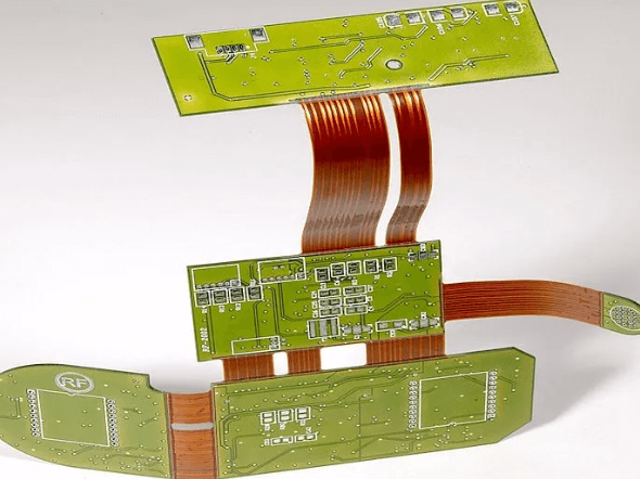
Rigid flex pcb design rules
Rigid flex pcb design rules
When designing a rigid-flex PCB stack-up, several key considerations must be taken into account to ensure optimal performance and reliability.
One of the primary factors to consider is the material selection.
The choice of materials for both the rigid and flexible sections of the PCB is crucial, as it directly impacts the board’s mechanical and electrical properties. Typically, rigid sections are made from FR4, a common and cost-effective material, while the flexible sections use polyimide, known for its excellent flexibility and thermal stability. Ensuring compatibility between these materials is essential to prevent delamination and other mechanical failures.
Another important consideration is the layer stack-up configuration.
The stack-up design must balance the need for electrical performance with mechanical flexibility. This involves determining the number of layers, the arrangement of signal, power, and ground planes, and the placement of vias. Proper layer stack-up can minimize signal integrity issues such as crosstalk and electromagnetic interference (EMI). Additionally, the stack-up should be designed to distribute mechanical stress evenly across the board, particularly in the bend areas of the flexible sections. This helps to prevent cracking and other forms of mechanical degradation over time.
The bend radius of the flexible sections is another critical factor.
The bend radius should be carefully calculated to avoid excessive stress on the copper traces and the polyimide substrate. A general rule of thumb is to maintain a bend radius that is at least ten times the thickness of the flexible section. This ensures that the board can bend without causing damage to the conductive traces or the insulating material. Furthermore, it is advisable to avoid placing vias and other critical components in the bend areas, as these can be points of mechanical weakness.
Thermal management is also a key consideration in rigid-flex PCB design.
The combination of rigid and flexible materials can create thermal expansion mismatches, leading to potential reliability issues. Proper thermal management techniques, such as the use of thermal vias and heat sinks, can help to dissipate heat effectively and maintain the integrity of the board. Additionally, the choice of materials with similar coefficients of thermal expansion (CTE) can mitigate the risks associated with thermal cycling.
Signal integrity is another aspect that cannot be overlooked.
The transition between rigid and flexible sections can introduce impedance discontinuities, which can affect high-speed signal transmission. Careful design of the trace widths, spacing, and routing can help to maintain consistent impedance and minimize signal reflection and loss. It is also important to consider the use of controlled impedance traces and differential pairs for high-speed signals to ensure signal integrity.
Manufacturability is a practical consideration that must be addressed early in the design process.
The complexity of rigid-flex PCBs can pose challenges in fabrication and assembly. Collaborating with experienced manufacturers can provide valuable insights into design for manufacturability (DFM) guidelines, helping to avoid common pitfalls and ensuring a smooth production process. This includes considerations such as panelization, solder mask application, and the selection of appropriate surface finishes.
In conclusion, designing a rigid-flex PCB stack-up requires a comprehensive understanding of material properties, mechanical and electrical design principles, thermal management, signal integrity, and manufacturability. By carefully considering these factors and employing best practices, designers can create robust and reliable rigid-flex PCBs that meet the demands of modern electronic applications.
Best Practices For Trace Routing In Rigid-Flex PCBs
When designing rigid-flex printed circuit boards (PCBs), adhering to best practices for trace routing is crucial to ensure the reliability and functionality of the final product. Rigid-flex PCBs combine the benefits of both rigid and flexible circuits, offering enhanced design versatility and improved performance in complex electronic applications. However, the unique characteristics of these hybrid boards necessitate careful consideration of trace routing to mitigate potential issues such as signal integrity problems, mechanical stress, and manufacturing challenges.
To begin with, it is essential to understand the importance of maintaining proper trace width and spacing.
In rigid-flex PCBs, traces must be designed to accommodate the varying mechanical properties of both rigid and flexible sections. Ensuring adequate trace width helps to prevent issues such as excessive current density, which can lead to overheating and potential failure. Similarly, maintaining appropriate spacing between traces is vital to avoid short circuits and crosstalk, which can degrade signal integrity. Designers should refer to industry standards and manufacturer guidelines to determine the optimal trace width and spacing for their specific application.
Transitioning from rigid to flexible sections requires special attention to trace routing.
It is advisable to avoid sharp bends and acute angles in the flexible regions, as these can introduce mechanical stress and increase the risk of trace cracking or delamination. Instead, designers should use smooth, gradual curves to distribute stress more evenly across the flex area. Additionally, staggering the traces in the flexible section can help to further reduce stress concentration and enhance the overall durability of the PCB.
Another critical aspect of trace routing in rigid-flex PCBs is the management of signal integrity.
High-speed signals are particularly susceptible to issues such as impedance discontinuities and electromagnetic interference (EMI). To mitigate these problems, designers should ensure that traces are routed with controlled impedance, especially in the flexible sections where variations in dielectric properties can occur. Utilizing ground planes and maintaining consistent trace geometry can help to achieve the desired impedance and minimize signal degradation.
Furthermore, it is important to consider the impact of via placement on trace routing.
Vias are used to connect traces between different layers of the PCB, but their placement can significantly affect the mechanical and electrical performance of the board. In rigid-flex designs, vias should be strategically placed to avoid areas of high mechanical stress, such as bend regions. Blind and buried vias can be employed to reduce the number of through-hole vias, thereby minimizing potential weak points in the flexible sections.
Thermal management is another crucial factor in trace routing for rigid-flex PCBs.
The combination of rigid and flexible materials can result in varying thermal expansion rates, which can cause mechanical stress and affect the reliability of the board. Designers should ensure that traces are routed in a manner that allows for efficient heat dissipation, particularly in areas with high power density. Utilizing thermal vias and heat sinks can help to manage heat effectively and prevent thermal-related issues.
In conclusion, best practices for trace routing in rigid-flex PCBs involve a comprehensive approach that addresses mechanical, electrical, and thermal considerations. By maintaining proper trace width and spacing, avoiding sharp bends, managing signal integrity, strategically placing vias, and ensuring effective thermal management, designers can create robust and reliable rigid-flex PCBs that meet the demands of modern electronic applications. Adhering to these guidelines not only enhances the performance of the PCB but also contributes to the overall success of the final product.
Material Selection Guidelines For Rigid-Flex PCB Manufacturing
When embarking on the design and manufacturing of rigid-flex printed circuit boards (PCBs), the selection of materials is a critical step that significantly influences the performance, reliability, and cost-effectiveness of the final product. The unique structure of rigid-flex PCBs, which combines rigid and flexible substrates, necessitates a careful consideration of various material properties to ensure optimal functionality. To begin with, the choice of base materials for both the rigid and flexible sections is paramount. Typically, the rigid sections are constructed from FR-4, a widely used glass-reinforced epoxy laminate known for its excellent mechanical strength and electrical insulation properties. However, the flexible sections require materials that can withstand repeated bending and flexing without compromising their integrity. Polyimide films, such as Kapton, are commonly used for this purpose due to their exceptional thermal stability, chemical resistance, and flexibility.
Transitioning from the base materials, the selection of adhesives is another crucial aspect.
Adhesives are used to bond the flexible layers to the rigid sections, and their performance directly impacts the durability and reliability of the PCB. Thermosetting adhesives, such as epoxy and acrylic, are often preferred for their strong bonding capabilities and resistance to environmental stressors. It is essential to choose adhesives that can endure the thermal cycles and mechanical stresses encountered during both the manufacturing process and the operational life of the PCB.
Furthermore, the choice of copper foil for the conductive layers is a vital consideration.
The copper used in rigid-flex PCBs must exhibit excellent ductility to accommodate the bending and flexing of the flexible sections without cracking or delaminating. Rolled annealed (RA) copper is typically favored over electro-deposited (ED) copper for its superior flexibility and fatigue resistance. The thickness of the copper foil also plays a significant role, with thinner foils being more suitable for flexible sections to enhance their bendability.
In addition to the primary materials, the selection of coverlays and solder masks is essential for protecting the circuitry and ensuring long-term reliability.
Coverlays, usually made from polyimide films, are applied to the flexible sections to shield the copper traces from environmental factors and mechanical damage. Solder masks, on the other hand, are used on the rigid sections to prevent solder bridging and protect the PCB during soldering processes. The compatibility of these protective layers with the underlying materials and their ability to withstand the thermal and mechanical stresses of the application are critical factors in their selection.
Moreover, the thermal management of rigid-flex PCBs is a significant consideration, particularly in high-performance applications.
The materials chosen must have appropriate thermal conductivity to dissipate heat effectively and prevent hotspots that could lead to component failure. This is especially important in applications such as aerospace, automotive, and medical devices, where reliability and performance are paramount.
Lastly, the environmental and regulatory compliance of the materials used in rigid-flex PCBs cannot be overlooked.
Materials must meet industry standards and regulations, such as RoHS (Restriction of Hazardous Substances) and REACH (Registration, Evaluation, Authorization, and Restriction of Chemicals), to ensure they are safe for use and environmentally friendly. This compliance not only ensures the safety and sustainability of the product but also facilitates its acceptance in global markets.
In conclusion, the material selection for rigid-flex PCB manufacturing is a multifaceted process that requires a thorough understanding of the properties and performance characteristics of various materials. By carefully considering factors such as mechanical strength, flexibility, thermal stability, and regulatory compliance, designers can ensure the production of high-quality, reliable, and cost-effective rigid-flex PCBs that meet the demands of their specific applications.
Design Rule Checks (DRC) For Ensuring Rigid-Flex PCB Reliability
Design Rule Checks (DRC) are essential for ensuring the reliability of rigid-flex printed circuit boards (PCBs). These checks serve as a critical step in the design process, helping to identify potential issues that could compromise the functionality and durability of the final product. By adhering to stringent design rules, engineers can mitigate risks and enhance the performance of rigid-flex PCBs, which are increasingly used in complex electronic applications due to their versatility and space-saving benefits.
One of the primary considerations in DRC for rigid-flex PCBs is the management of mechanical stress.
The flexible sections of these boards are particularly susceptible to stress, which can lead to cracking or delamination if not properly addressed. To prevent such issues, it is crucial to follow guidelines on bend radius, which dictate the minimum radius that the flexible part of the PCB can be bent without causing damage. Typically, a larger bend radius is recommended to reduce stress concentration, thereby enhancing the board’s longevity.
In addition to mechanical stress, electrical performance is another critical aspect that DRC aims to safeguard.
Ensuring proper trace width and spacing is vital to prevent issues such as signal interference and crosstalk. These parameters are especially important in high-frequency applications where even minor deviations can lead to significant performance degradation. By adhering to the specified trace width and spacing rules, designers can maintain signal integrity and ensure reliable operation of the PCB.
Thermal management is another key factor addressed by DRC in rigid-flex PCB design.
The combination of rigid and flexible materials can create thermal expansion mismatches, which may lead to warping or other thermal-related failures. To mitigate these risks, it is essential to consider the thermal properties of the materials used and ensure adequate heat dissipation. This can be achieved through the strategic placement of thermal vias and the use of appropriate materials that can withstand the operating temperature range of the application.
Furthermore, DRC also encompasses the verification of layer stack-up and material selection.
The layer stack-up must be carefully designed to balance the mechanical and electrical requirements of the PCB. This involves selecting the right combination of rigid and flexible layers, as well as ensuring proper adhesion between them. Material selection is equally important, as the materials used must be compatible with the intended application and capable of withstanding the environmental conditions they will be exposed to.
Another critical aspect of DRC is the inspection of via structures.
Vias are used to establish electrical connections between different layers of the PCB, and their reliability is paramount. In rigid-flex designs, vias that transition between rigid and flexible sections require special attention. These vias must be designed to accommodate the mechanical stresses associated with bending and flexing, which can be achieved through the use of reinforced vias or other specialized via structures.
Lastly, DRC involves the verification of manufacturing tolerances.
Rigid-flex PCBs often have tighter tolerances compared to traditional rigid PCBs due to their complex structure. Ensuring that the design adheres to the manufacturing capabilities of the chosen fabrication process is crucial to avoid issues during production. This includes verifying the accuracy of dimensions, hole sizes, and other critical features.
In conclusion, Design Rule Checks are indispensable for ensuring the reliability of rigid-flex PCBs. By addressing mechanical stress, electrical performance, thermal management, layer stack-up, via structures, and manufacturing tolerances, DRC helps to identify and mitigate potential issues early in the design process. This not only enhances the performance and durability of the final product but also reduces the likelihood of costly rework and delays during manufacturing.