What is 6 layer pcb
What is 6 layer pcb
A 6-layer printed circuit board (PCB) is a sophisticated and highly efficient type of PCB that is widely used in various advanced electronic applications.
Unlike simpler single-layer or double-layer PCBs, a 6-layer PCB consists of six layers of conductive material, typically copper, separated by insulating layers. This multi-layer structure allows for greater complexity and functionality in electronic circuits, making it an essential component in modern electronics.
To understand the structure of a 6-layer PCB, it is important to first grasp the basic concept of a PCB.
A PCB is a board that mechanically supports and electrically connects electronic components using conductive pathways, or traces, etched from copper sheets laminated onto a non-conductive substrate. In a 6-layer PCB, these conductive pathways are distributed across six distinct layers, which are stacked and bonded together. The layers are typically arranged in a specific sequence to optimize performance and minimize interference.
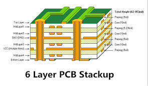
The typical structure of a 6-layer PCB includes two outer layers, which are often used for component placement and routing of critical signals.
These outer layers are followed by two inner signal layers, which are primarily used for routing additional signals that cannot be accommodated on the outer layers. Finally, there are two inner layers dedicated to power and ground planes. The power plane provides a stable voltage supply to the components, while the ground plane serves as a reference point for the circuit and helps to reduce electromagnetic interference (EMI).
One of the primary benefits of a 6-layer PCB is its ability to support higher component density and more complex circuitry.
By distributing the traces across multiple layers, designers can create more intricate and compact designs without compromising performance. This is particularly advantageous in applications where space is limited, such as in smartphones, medical devices, and aerospace electronics.
Moreover, the use of dedicated power and ground planes in a 6-layer PCB significantly enhances signal integrity and reduces noise.
The ground plane acts as a shield, protecting the signal traces from external EMI and minimizing crosstalk between adjacent traces. This results in cleaner signal transmission and improved overall performance of the electronic device.
Another notable advantage of a 6-layer PCB is its improved thermal management.
The additional layers provide more surface area for heat dissipation, which is crucial in high-power applications. Efficient thermal management helps to prevent overheating and ensures the reliability and longevity of the electronic components.
Furthermore, the flexibility offered by a 6-layer PCB allows for more efficient routing of signals.
Designers can strategically place critical signals on the inner layers, away from potential sources of interference, while using the outer layers for less critical routing. This flexibility not only simplifies the design process but also enhances the overall performance of the circuit.
In conclusion, a 6-layer PCB is a highly versatile and efficient solution for modern electronic applications. Its multi-layer structure allows for greater complexity, improved signal integrity, and better thermal management, making it an ideal choice for high-performance and space-constrained designs. As technology continues to advance, the demand for multi-layer PCBs, including 6-layer variants, is expected to grow, further solidifying their importance in the electronics industry.
Design Considerations For 6 Layer PCBs
When designing a 6-layer printed circuit board (PCB), several critical considerations must be taken into account to ensure optimal performance and reliability. A 6-layer PCB typically consists of six conductive layers, including signal layers, power planes, and ground planes, which are laminated together with insulating material. This configuration offers a balance between complexity and cost, making it suitable for a wide range of applications, from consumer electronics to industrial equipment.
One of the primary design considerations for a 6-layer PCB is the stack-up configuration.
The stack-up determines the arrangement of the conductive and insulating layers, which directly impacts the board’s electrical performance, signal integrity, and electromagnetic compatibility (EMC). A common stack-up for a 6-layer PCB includes two outer signal layers, two inner signal layers, and two internal planes, typically designated as power and ground planes. This configuration helps to minimize signal crosstalk and electromagnetic interference (EMI) by providing effective shielding and a low-impedance return path for high-speed signals.
Another crucial aspect of 6-layer PCB design is the selection of materials.
The choice of substrate material, such as FR4, polyimide, or Rogers, affects the board’s thermal and mechanical properties, as well as its electrical performance. For high-frequency applications, materials with low dielectric constant (Dk) and low dissipation factor (Df) are preferred to reduce signal loss and maintain signal integrity. Additionally, the thickness of the copper layers must be carefully chosen to handle the required current-carrying capacity while maintaining manufacturability and cost-effectiveness.
Signal integrity is a key concern in 6-layer PCB design, particularly for high-speed digital and RF circuits.
To mitigate signal degradation, designers must pay close attention to trace impedance control, differential pair routing, and via placement. Controlled impedance traces ensure consistent signal propagation and reduce reflections, which can cause data errors. Differential pairs, used for high-speed data transmission, must be routed with precise spacing and length matching to maintain signal integrity. Vias, which connect different layers of the PCB, should be minimized in high-speed signal paths to reduce signal distortion and maintain signal quality.
Thermal management is another important consideration in 6-layer PCB design.
As electronic components become more powerful and compact, effective heat dissipation becomes critical to prevent overheating and ensure reliable operation. Designers can incorporate thermal vias, heat sinks, and copper pours to enhance heat dissipation. Additionally, careful placement of components and power planes can help distribute heat more evenly across the board.
Manufacturability and cost are also significant factors in 6-layer PCB design.
While a 6-layer PCB offers improved performance and reliability compared to simpler designs, it also involves more complex fabrication processes and higher material costs. Designers must work closely with PCB manufacturers to ensure that the design can be produced efficiently and within budget. This includes considering factors such as minimum trace width and spacing, via sizes, and layer-to-layer registration tolerances.
In conclusion, designing a 6-layer PCB requires careful consideration of stack-up configuration, material selection, signal integrity, thermal management, and manufacturability. By addressing these factors, designers can create PCBs that meet the performance, reliability, and cost requirements of their specific applications. As technology continues to advance, the demand for multi-layer PCBs will likely grow, making it essential for designers to stay informed about best practices and emerging trends in PCB design.
Applications Of 6 Layer PCBs In Modern Electronics
A 6-layer printed circuit board (PCB) is a sophisticated and versatile component in modern electronics, offering enhanced functionality and performance compared to simpler PCB designs. These multi-layered boards are constructed by stacking six layers of conductive material, typically copper, separated by insulating layers. This intricate design allows for more complex circuitry and greater density of components, making 6-layer PCBs indispensable in various advanced applications.
One of the primary applications of 6-layer PCBs is in the telecommunications industry.
As the demand for faster and more reliable communication networks grows, the need for high-performance PCBs becomes increasingly critical. 6-layer PCBs are commonly used in the construction of routers, switches, and other networking equipment. Their multi-layer design enables the integration of high-speed signal transmission lines and power distribution networks, ensuring efficient and stable performance. Additionally, the ability to incorporate multiple ground and power planes helps to minimize electromagnetic interference (EMI), which is crucial for maintaining signal integrity in high-frequency applications.
In the realm of consumer electronics, 6-layer PCBs are frequently employed in the design of smartphones, tablets, and laptops.
These devices require compact and lightweight components that can support a multitude of functions, from processing power to connectivity. The multi-layer structure of 6-layer PCBs allows for the integration of complex circuits within a small footprint, making them ideal for portable electronic devices. Furthermore, the additional layers provide more routing options, which can help to reduce the overall size and weight of the final product. This is particularly important in the competitive consumer electronics market, where manufacturers are constantly striving to create thinner and lighter devices.
The automotive industry also benefits significantly from the use of 6-layer PCBs.
Modern vehicles are equipped with a wide array of electronic systems, including advanced driver-assistance systems (ADAS), infotainment systems, and engine control units (ECUs). These systems require reliable and high-performance PCBs to function effectively. The multi-layer design of 6-layer PCBs allows for the integration of complex circuitry and power distribution networks, ensuring that these critical systems operate smoothly and efficiently. Moreover, the ability to incorporate multiple ground and power planes helps to reduce EMI, which is essential for maintaining the reliability and safety of automotive electronics.
In the field of medical devices, 6-layer PCBs play a crucial role in the development of advanced diagnostic and therapeutic equipment.
Medical devices such as MRI machines, ultrasound equipment, and portable monitoring devices require highly reliable and precise electronic components. The multi-layer structure of 6-layer PCBs allows for the integration of complex circuits and high-density interconnections, ensuring accurate and reliable performance. Additionally, the ability to incorporate multiple ground and power planes helps to minimize EMI, which is vital for maintaining the accuracy and safety of medical devices.
The aerospace industry also relies on 6-layer PCBs for the development of advanced avionics systems and satellite communication equipment.
These applications demand high-performance and reliable electronic components that can withstand harsh environmental conditions. The multi-layer design of 6-layer PCBs allows for the integration of complex circuitry and power distribution networks, ensuring efficient and stable performance in demanding aerospace applications. Furthermore, the ability to incorporate multiple ground and power planes helps to reduce EMI, which is crucial for maintaining signal integrity in high-frequency applications.
In conclusion, 6-layer PCBs are essential components in a wide range of modern electronic applications, from telecommunications and consumer electronics to automotive, medical, and aerospace industries. Their multi-layer design allows for the integration of complex circuitry and high-density interconnections, ensuring efficient and reliable performance in demanding applications. As technology continues to advance, the importance of 6-layer PCBs in modern electronics is only expected to grow.
Manufacturing Process Of 6 Layer PCBs: A Step-By-Step Guide
The manufacturing process of a 6-layer printed circuit board (PCB) is a complex and intricate procedure that requires precision and expertise. This multi-layered structure is essential for advanced electronic devices, providing enhanced functionality and performance. To understand the manufacturing process, it is crucial to delve into each step, from the initial design to the final inspection.
The journey begins with the design phase, where engineers use specialized software to create a detailed blueprint of the PCB.
This design includes the layout of all six layers, specifying the placement of components, traces, and vias. Once the design is finalized, it is converted into a format suitable for manufacturing, typically Gerber files. These files serve as the digital instructions for the subsequent steps.
Following the design phase, the manufacturing process moves to the fabrication of the individual layers.
Each layer starts with a substrate, usually made of fiberglass-reinforced epoxy laminate, known as FR4. A thin layer of copper is laminated onto both sides of the substrate. The copper is then coated with a photosensitive material called photoresist. Using ultraviolet light, the photoresist is exposed through a mask that corresponds to the desired copper pattern. The exposed areas harden, while the unexposed areas remain soft and are subsequently washed away, revealing the copper underneath.
The next step involves etching, where the exposed copper is removed using a chemical solution, leaving behind the desired copper traces. This process is repeated for each of the six layers, ensuring that each layer has the correct pattern of copper traces. Once all the layers are etched, they are aligned and laminated together under high pressure and temperature, forming a single, cohesive board.
After lamination, the board undergoes drilling to create holes for vias and through-hole components.
These holes are precisely drilled using computer-controlled machines to ensure accuracy. The drilled holes are then plated with copper to establish electrical connections between the layers. This process, known as electroplating, involves immersing the board in a copper sulfate solution and applying an electric current, which deposits a thin layer of copper onto the walls of the holes.
With the vias and through-holes in place, the next step is to apply a solder mask.
This protective layer is applied to both sides of the board, covering the copper traces and leaving only the pads and holes exposed. The solder mask prevents solder bridges and short circuits during the assembly process. Once the solder mask is applied, a silkscreen layer is added, which includes component labels, logos, and other markings to aid in assembly and troubleshooting.
The final stages of the manufacturing process involve surface finish and testing.
The surface finish, such as HASL (Hot Air Solder Leveling) or ENIG (Electroless Nickel Immersion Gold), is applied to the exposed copper pads to enhance solderability and protect against oxidation. The board then undergoes rigorous testing, including electrical tests to verify continuity and insulation resistance, as well as visual inspections to check for defects.
In conclusion, the manufacturing process of a 6-layer PCB is a meticulous and multi-faceted procedure that demands precision at every step. From the initial design to the final inspection, each phase is crucial in ensuring the functionality and reliability of the finished product. This intricate process enables the creation of advanced electronic devices that are integral to modern technology.