Flex pcb trace width
Importance Of Trace Width In Flex PCB Design
In the realm of flexible printed circuit boards (flex PCBs), the trace width is a critical parameter that significantly influences the performance, reliability, and manufacturability of the final product.
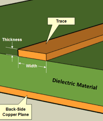
The trace width, which refers to the width of the conductive paths that carry electrical signals, must be meticulously designed to ensure optimal functionality.
Understanding the importance of trace width in flex PCB design is essential for engineers and designers aiming to create high-quality, durable, and efficient electronic devices.
One of the primary reasons trace width is so crucial in flex PCB design is its direct impact on electrical performance.
The width of the traces determines the amount of current they can safely carry without overheating. If the trace width is too narrow, it can lead to excessive resistance, resulting in voltage drops and potential signal integrity issues. Conversely, overly wide traces can occupy unnecessary space, limiting the flexibility and compactness that are often the primary advantages of using flex PCBs. Therefore, achieving the right balance in trace width is vital to maintaining the electrical performance and efficiency of the circuit.
Moreover, the trace width also affects the thermal management of the flex PCB.
As electrical current flows through the traces, it generates heat. Narrow traces can exacerbate this issue by concentrating the heat in a smaller area, which can lead to thermal stress and potential damage to the PCB and its components. On the other hand, appropriately sized traces can help dissipate heat more effectively, enhancing the overall thermal stability of the circuit. This is particularly important in applications where the flex PCB is subjected to varying environmental conditions or where high power levels are involved.
In addition to electrical and thermal considerations, the mechanical properties of the flex PCB are also influenced by trace width.
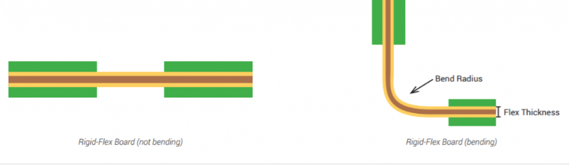
Flex PCBs are often used in applications where the circuit needs to bend, twist, or fold. In such scenarios, the mechanical integrity of the traces becomes paramount. Traces that are too narrow may be prone to cracking or breaking under mechanical stress, compromising the reliability of the circuit. Conversely, traces that are too wide may reduce the flexibility of the PCB, negating one of its key advantages. Therefore, careful consideration of trace width is essential to ensure that the flex PCB can withstand the mechanical demands of its intended application.
Furthermore, manufacturability is another critical aspect affected by trace width.
The precision required to fabricate narrow traces can increase the complexity and cost of the manufacturing process. Advanced techniques and equipment may be necessary to achieve the desired trace width, which can impact production timelines and budgets. By optimizing trace width, designers can strike a balance between performance requirements and manufacturing feasibility, ensuring that the flex PCB can be produced efficiently and cost-effectively.
In conclusion, the importance of trace width in flex PCB design cannot be overstated. It plays a pivotal role in determining the electrical performance, thermal management, mechanical integrity, and manufacturability of the circuit. By carefully considering and optimizing trace width, designers can create flex PCBs that meet the stringent demands of modern electronic applications, ensuring reliability, efficiency, and durability. As technology continues to advance, the significance of precise trace width design will only become more pronounced, underscoring its critical role in the development of next-generation flexible electronic devices.
Calculating Optimal Trace Width For Flex PCBs
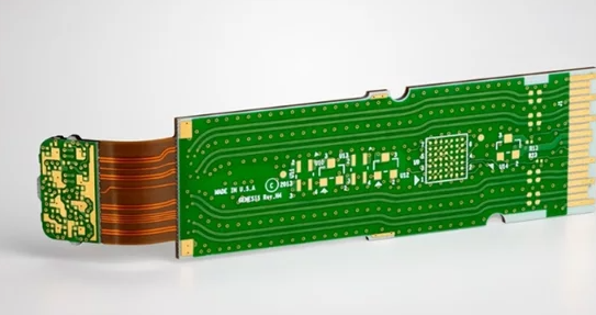
Calculating the optimal trace width for flexible printed circuit boards (flex PCBs) is a critical aspect of PCB design that ensures both functionality and reliability. Flex PCBs, known for their ability to bend and twist, are increasingly used in applications where space constraints and mechanical flexibility are paramount. To achieve optimal performance, designers must carefully consider the trace width, which directly impacts the electrical and thermal characteristics of the circuit.
The first step in determining the appropriate trace width is to understand the current-carrying capacity of the traces.
The current-carrying capacity is influenced by the trace width, thickness, and the material properties of the flex PCB. IPC-2223, a standard for flex PCB design, provides guidelines for calculating the current-carrying capacity. According to this standard, the trace width must be sufficient to handle the expected current without causing excessive temperature rise, which could lead to thermal degradation of the flex material and potential failure of the circuit.
In addition to current-carrying capacity, signal integrity is another crucial factor to consider.
Signal integrity refers to the preservation of the signal’s quality as it travels through the trace. Narrow traces can lead to increased resistance and inductance, which can distort high-frequency signals. Therefore, for high-speed applications, wider traces are often preferred to minimize signal loss and maintain signal integrity. However, the available space on the flex PCB may limit the trace width, necessitating a careful balance between trace width and signal performance.
Thermal management is also a significant consideration in flex PCB design.
As current flows through the traces, it generates heat, which must be dissipated to prevent damage to the flex material and other components. Wider traces have a larger surface area, which helps in better heat dissipation. However, the flexibility of the PCB can be compromised if the traces are too wide, as they can restrict the bending and twisting capabilities of the flex PCB. Therefore, designers must optimize the trace width to ensure adequate thermal management while maintaining the desired flexibility.
Moreover, the manufacturing process and material properties of the flex PCB play a vital role in determining the optimal trace width.
Flex PCBs are typically made from polyimide or polyester materials, which have different thermal and mechanical properties compared to rigid PCBs. The adhesion of the copper traces to the flex material is also a critical factor, as poor adhesion can lead to delamination and circuit failure. Therefore, designers must work closely with manufacturers to understand the limitations and capabilities of the materials and processes used in flex PCB fabrication.
Furthermore, environmental factors such as temperature, humidity, and mechanical stress must be considered when calculating the trace width.
Flex PCBs are often used in harsh environments where they are subjected to extreme temperatures and mechanical stress. These conditions can affect the electrical and mechanical properties of the traces, necessitating a more robust design with wider traces to ensure reliability.
In conclusion, calculating the optimal trace width for flex PCBs involves a comprehensive analysis of current-carrying capacity, signal integrity, thermal management, manufacturing processes, and environmental factors. By carefully considering these aspects, designers can ensure that the flex PCB meets the required performance and reliability standards while maintaining the desired flexibility. This meticulous approach not only enhances the functionality of the flex PCB but also extends its lifespan, making it a crucial element in the design of modern electronic devices.
Common Mistakes In Flex PCB Trace Width Selection
Selecting the appropriate trace width for flexible printed circuit boards (flex PCBs) is a critical aspect of PCB design that can significantly impact the performance, reliability, and manufacturability of the final product. However, several common mistakes are often made during this process, which can lead to suboptimal outcomes.
One prevalent error is underestimating the current-carrying capacity of the traces.
Designers sometimes choose trace widths that are too narrow to handle the required current, leading to excessive heat generation and potential failure of the circuit. It is essential to consider the current requirements and use appropriate design guidelines to ensure that the trace width can handle the expected load without overheating.
Another frequent mistake is neglecting the impact of environmental factors on trace width.
Flex PCBs are often used in applications where they are subjected to varying temperatures, humidity levels, and mechanical stresses. These environmental conditions can affect the electrical and mechanical properties of the traces. For instance, high temperatures can increase the resistance of the traces, while mechanical stresses can cause cracks or delamination. Therefore, it is crucial to account for these factors during the design phase and select trace widths that can withstand the anticipated environmental conditions.
In addition to environmental considerations, designers sometimes overlook the importance of manufacturing tolerances.
Flex PCBs are typically produced using processes that have inherent variations, such as etching and plating. These variations can result in trace widths that are narrower or wider than intended. Failing to account for these manufacturing tolerances can lead to issues such as short circuits or open circuits. To mitigate this risk, it is advisable to work closely with the PCB manufacturer and incorporate appropriate tolerances into the design.
Furthermore, the choice of materials can also influence the selection of trace width.
Different materials have varying electrical and thermal properties, which can affect the performance of the traces. For example, using a material with higher thermal conductivity can help dissipate heat more effectively, allowing for narrower trace widths. Conversely, materials with lower thermal conductivity may require wider traces to prevent overheating. It is important to select materials that are compatible with the intended application and to adjust the trace width accordingly.
Another common mistake is failing to consider the impact of signal integrity on trace width selection.
High-frequency signals can be particularly sensitive to trace width variations, which can cause signal degradation and interference. To maintain signal integrity, it is important to use controlled impedance traces and to carefully design the trace width and spacing. This may involve using simulation tools to model the signal behavior and optimize the trace dimensions.
Lastly, designers sometimes make the mistake of not thoroughly testing and validating their designs.
Even with careful planning and consideration of all relevant factors, it is possible for issues to arise during the manufacturing and assembly process. Conducting thorough testing and validation can help identify and address any potential problems before the final product is produced. This may involve using techniques such as thermal imaging, electrical testing, and mechanical stress testing to ensure that the traces perform as expected under real-world conditions.
In conclusion, selecting the appropriate trace width for flex PCBs is a complex process that requires careful consideration of various factors, including current-carrying capacity, environmental conditions, manufacturing tolerances, material properties, signal integrity, and thorough testing. By avoiding common mistakes and taking a comprehensive approach to trace width selection, designers can enhance the performance, reliability, and manufacturability of their flex PCB designs.
Impact Of Trace Width On Flex PCB Performance
The impact of trace width on the performance of flexible printed circuit boards (flex PCBs) is a critical consideration in the design and manufacturing process. Flex PCBs are increasingly utilized in various applications due to their ability to bend, fold, and conform to complex shapes, making them ideal for compact and dynamic electronic devices. However, the trace width, which refers to the width of the conductive pathways on the PCB, plays a significant role in determining the overall performance, reliability, and functionality of these circuits.
One of the primary factors influenced by trace width is the electrical resistance of the circuit.
Wider traces typically exhibit lower resistance, which is advantageous for high-current applications. Lower resistance minimizes power loss and heat generation, thereby enhancing the efficiency and longevity of the PCB. Conversely, narrower traces have higher resistance, which can lead to increased power dissipation and potential overheating issues. Therefore, selecting an appropriate trace width is essential to ensure optimal electrical performance and thermal management.
In addition to electrical resistance, the trace width also affects the signal integrity of the flex PCB.
High-frequency signals are particularly sensitive to variations in trace width, as these can cause impedance mismatches and signal reflections. Such issues can degrade the quality of the transmitted signals, leading to data errors and reduced performance in high-speed communication systems. By carefully controlling the trace width, designers can maintain consistent impedance and minimize signal degradation, thereby ensuring reliable data transmission.
Moreover, the mechanical properties of flex PCBs are also influenced by trace width.
Flex PCBs are often subjected to repeated bending and flexing, which can induce mechanical stress on the traces. Wider traces are generally more robust and can better withstand mechanical deformation without cracking or breaking. On the other hand, narrower traces are more susceptible to mechanical failure, especially in applications involving frequent or severe flexing. Therefore, optimizing trace width is crucial for enhancing the mechanical durability and reliability of flex PCBs.
Thermal management is another aspect where trace width plays a pivotal role.
Wider traces can dissipate heat more effectively, which is particularly important in high-power applications. Efficient heat dissipation helps prevent localized hotspots and ensures uniform temperature distribution across the PCB. This not only improves the performance and reliability of the electronic components but also extends the overall lifespan of the flex PCB. In contrast, narrower traces may struggle to dissipate heat adequately, leading to thermal stress and potential damage to the PCB and its components.
Furthermore, the manufacturability of flex PCBs is also impacted by trace width.
Advanced fabrication techniques are required to produce narrow traces with high precision, which can increase manufacturing complexity and cost. Wider traces, being easier to fabricate, can simplify the production process and reduce costs. However, the choice of trace width must balance manufacturability with the specific performance requirements of the application.
In conclusion, the trace width of flex PCBs significantly influences their electrical, mechanical, and thermal performance. Wider traces offer lower resistance, better signal integrity, enhanced mechanical durability, and improved thermal management, making them suitable for high-current and high-power applications. Conversely, narrower traces, while more challenging to manufacture, may be necessary for applications requiring high-density interconnections. Therefore, careful consideration of trace width is essential in the design and manufacturing of flex PCBs to ensure optimal performance and reliability in their intended applications.