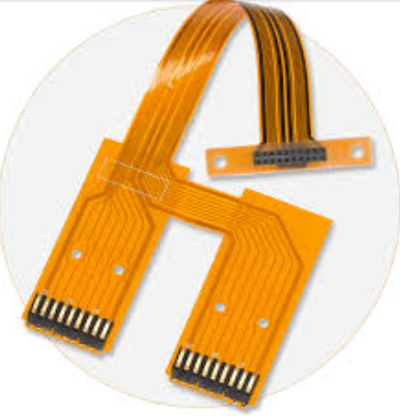
Printing flexible pcb
Advantages Of Printing Flexible PCBs For Modern Electronics
Printing flexible PCBs (Printed Circuit Boards) has become an increasingly popular method in the realm of modern electronics, offering a multitude of advantages that cater to the evolving demands of contemporary technology.
One of the primary benefits of flexible PCBs is their inherent adaptability.
Unlike traditional rigid PCBs, flexible PCBs can be bent, folded, and twisted to fit into compact and irregularly shaped spaces. This flexibility is particularly advantageous in the design of wearable devices, medical implants, and other applications where space constraints are a significant consideration.
Moreover, the lightweight nature of flexible PCBs contributes to the overall reduction in the weight of electronic devices.
This is especially critical in the development of portable electronics such as smartphones, tablets, and laptops, where every gram counts. The reduction in weight not only enhances the user experience but also improves the energy efficiency of the devices, as less power is required to operate lighter components.
In addition to their physical flexibility and lightweight properties, flexible PCBs offer superior durability and reliability.
The materials used in the construction of flexible PCBs, such as polyimide or polyester films, are known for their excellent thermal stability and resistance to harsh environmental conditions. This makes flexible PCBs ideal for use in automotive, aerospace, and industrial applications, where they are often subjected to extreme temperatures, vibrations, and mechanical stresses.
Another significant advantage of printing flexible PCBs is the potential for cost savings in both manufacturing and assembly processes.
The ability to print circuits directly onto flexible substrates reduces the need for multiple layers and complex interconnections, thereby simplifying the overall design and manufacturing process. This not only lowers production costs but also minimizes the likelihood of errors and defects, leading to higher yields and improved product quality.
Furthermore, the use of flexible PCBs can lead to enhanced performance and functionality of electronic devices.
The flexibility allows for more efficient use of space within the device, enabling the integration of additional components and features without increasing the overall size. This is particularly beneficial in the development of advanced technologies such as flexible displays, foldable smartphones, and other innovative consumer electronics that require a high degree of design versatility.
The environmental impact of flexible PCBs is also worth noting.
The materials used in flexible PCBs are often more environmentally friendly compared to those used in traditional rigid PCBs. Additionally, the reduction in material usage and waste during the manufacturing process contributes to a lower environmental footprint. This aligns with the growing emphasis on sustainability and eco-friendly practices within the electronics industry.
In conclusion, the advantages of printing flexible PCBs for modern electronics are manifold. Their adaptability, lightweight nature, durability, cost-effectiveness, enhanced performance, and environmental benefits make them an attractive option for a wide range of applications. As technology continues to advance and the demand for more compact, efficient, and versatile electronic devices grows, the adoption of flexible PCBs is likely to become even more widespread. This trend underscores the importance of continued innovation and development in the field of flexible PCB technology, ensuring that it remains at the forefront of modern electronics design and manufacturing.

Step-By-Step Guide To Printing Flexible PCBs At Home
Printing flexible PCBs at home can be a rewarding endeavor for electronics enthusiasts and professionals alike. The process, while intricate, is manageable with the right tools and a methodical approach. This guide will walk you through the essential steps to successfully print flexible PCBs in the comfort of your own workspace.
To begin with, it is crucial to gather all necessary materials and equipment.
You will need a computer with PCB design software, a laser printer, a laminator, a UV exposure unit, a developer solution, etching solution, and flexible PCB substrate material. Additionally, ensure you have protective gear such as gloves and safety glasses, as some chemicals used in the process can be hazardous.
The first step involves designing your PCB layout using specialized software.
Programs like Eagle, KiCad, or Altium Designer are popular choices. Carefully plan your circuit, paying attention to the placement of components and the routing of traces. Once your design is complete, print the layout onto a transparency film using a laser printer. It is important to use a high-quality transparency film to ensure that the printed traces are sharp and clear.
Next, prepare the flexible PCB substrate.
Cut the substrate to the desired size, ensuring it is clean and free of any dust or debris. Place the printed transparency film onto the substrate, aligning it precisely. This step is critical, as any misalignment can result in faulty connections on the final PCB.
Following this, the substrate and transparency film need to be exposed to UV light.
Place them in a UV exposure unit, ensuring even exposure across the entire surface. The duration of exposure will depend on the specific photoresist material used on your flexible PCB substrate. Typically, this process takes a few minutes. After exposure, the photoresist will harden in the areas where the UV light has passed through the transparency film.
Once the exposure is complete, the next step is to develop the PCB.
Submerge the exposed substrate in a developer solution, which will remove the unexposed photoresist, revealing the copper traces. This process should be done carefully, following the manufacturer’s instructions for the developer solution. After development, rinse the substrate thoroughly with water to remove any remaining developer solution.
The subsequent step involves etching the PCB. Place the developed substrate into an etching solution, such as ferric chloride or ammonium persulfate.
The etching solution will dissolve the exposed copper, leaving behind only the desired copper traces protected by the hardened photoresist. Monitor the etching process closely to avoid over-etching, which can damage the traces. Once etching is complete, rinse the substrate with water to stop the etching process.
After etching, remove the remaining photoresist by using a suitable solvent or by gently scrubbing the substrate. This will reveal the final copper traces of your flexible PCB. Inspect the PCB carefully for any defects or incomplete traces. If necessary, use a multimeter to check for continuity and ensure all connections are intact.
Finally, the flexible PCB is ready for component placement and soldering.
Due to the nature of flexible PCBs, it is advisable to use low-temperature soldering techniques to avoid damaging the substrate. Carefully solder the components onto the PCB, ensuring secure and reliable connections.
In conclusion, printing flexible PCBs at home requires precision and attention to detail at each step. By following this guide and using the appropriate materials and equipment, you can successfully create high-quality flexible PCBs for your electronic projects.

Common Challenges And Solutions In Flexible PCB Printing
Printing flexible PCBs (Printed Circuit Boards) presents a unique set of challenges that differ significantly from those encountered in traditional rigid PCB manufacturing. One of the primary difficulties lies in the inherent flexibility of the substrate material, which can lead to issues such as warping, stretching, and misalignment during the printing process. These problems can result in defects that compromise the functionality and reliability of the final product. To address these challenges, manufacturers must employ specialized techniques and equipment designed to handle the delicate nature of flexible substrates.
A common issue in flexible PCB printing is the precise alignment of the layers.
Unlike rigid PCBs, flexible substrates can shift or stretch, making it difficult to maintain accurate registration between layers. This misalignment can cause short circuits or open circuits, leading to device failure. To mitigate this, manufacturers often use advanced alignment systems that employ optical recognition and automated adjustments to ensure precise layer registration. Additionally, the use of fiducial markers on the substrate can help in maintaining alignment throughout the printing process.
Another significant challenge is the selection of appropriate materials.
Flexible PCBs require substrates that can withstand bending and flexing without breaking or losing their electrical properties. Polyimide is a commonly used material due to its excellent thermal stability and mechanical strength. However, the choice of conductive inks and adhesives also plays a crucial role. These materials must be flexible enough to endure repeated bending while maintaining strong adhesion to the substrate. Manufacturers often conduct extensive testing to identify the best combination of materials that meet the specific requirements of their applications.
Thermal management is another critical aspect of flexible PCB printing.
The thin and flexible nature of these substrates makes them more susceptible to thermal stress during soldering and other high-temperature processes. Excessive heat can cause warping or delamination, leading to circuit failure. To address this, manufacturers may use low-temperature soldering techniques or employ heat sinks and thermal relief structures to dissipate heat more effectively. Additionally, careful control of the reflow soldering profile can help minimize thermal stress on the flexible substrate.
The printing process itself also poses challenges.
Screen printing, a common method for applying conductive inks, requires precise control to ensure uniform ink deposition. Variations in ink thickness can lead to inconsistent electrical performance and potential failure points. To achieve consistent results, manufacturers may use automated screen printing equipment with fine-tuned parameters for pressure, speed, and stencil design. Alternatively, inkjet printing offers a more precise method for depositing conductive inks, allowing for greater control over ink placement and thickness.
Quality control is paramount in flexible PCB manufacturing.
Given the delicate nature of the substrates and the potential for defects, rigorous inspection processes are essential. Automated optical inspection (AOI) systems can detect misalignments, incomplete circuits, and other defects early in the production process, allowing for timely corrections. Additionally, electrical testing ensures that the final product meets the required performance standards.
In conclusion, printing flexible PCBs involves navigating a range of challenges, from material selection and alignment to thermal management and precise ink deposition. By employing advanced technologies and rigorous quality control measures, manufacturers can overcome these obstacles and produce reliable, high-performance flexible PCBs. The continuous evolution of materials and printing techniques promises to further enhance the capabilities and applications of flexible PCBs in the future.
Innovations In Flexible PCB Printing Technology
The realm of electronics has witnessed remarkable advancements over the past few decades, and one of the most significant innovations is the development of flexible printed circuit boards (PCBs).
These flexible PCBs have revolutionized the way electronic devices are designed and manufactured, offering unprecedented versatility and functionality. The advent of flexible PCB printing technology has further propelled this innovation, enabling the production of highly adaptable and efficient electronic circuits.
Flexible PCBs, unlike their rigid counterparts, are made from materials that allow them to bend and flex without breaking.
This flexibility opens up a myriad of possibilities for electronic device design, particularly in applications where space constraints and dynamic movement are critical factors. For instance, flexible PCBs are extensively used in wearable technology, medical devices, and automotive applications, where traditional rigid PCBs would be impractical.
The process of printing flexible PCBs involves several sophisticated techniques that ensure precision and reliability.
One of the most notable advancements in this field is the use of additive manufacturing, commonly known as 3D printing. This technique allows for the layer-by-layer construction of the PCB, enabling intricate designs and complex geometries that were previously unattainable. By using conductive inks and substrates, manufacturers can create highly efficient and compact circuits that can conform to various shapes and surfaces.
Moreover, the integration of advanced materials has significantly enhanced the performance and durability of flexible PCBs.
Polyimide and polyester are among the most commonly used substrates due to their excellent thermal stability and mechanical properties. These materials not only provide the necessary flexibility but also ensure that the circuits can withstand harsh environmental conditions. Additionally, the development of conductive inks with improved conductivity and adhesion properties has further optimized the performance of flexible PCBs.
Another critical innovation in flexible PCB printing technology is the implementation of roll-to-roll (R2R) processing.
This method involves continuously feeding a flexible substrate through a series of printing and processing stations, allowing for high-speed and large-scale production. R2R processing is particularly advantageous for applications that require mass production, such as consumer electronics and automotive components. The ability to produce flexible PCBs in a continuous and automated manner significantly reduces manufacturing costs and time, making it a highly efficient solution for the industry.
Furthermore, advancements in laser direct structuring (LDS) have also contributed to the evolution of flexible PCB printing technology.
LDS enables the creation of fine and precise circuit patterns by using a laser to selectively activate a substrate, which is then metallized to form conductive traces. This technique offers exceptional design flexibility and accuracy, making it ideal for applications that demand high precision and miniaturization.
In addition to these technological advancements, the growing emphasis on sustainability has also influenced the development of flexible PCB printing technology.
Manufacturers are increasingly adopting eco-friendly materials and processes to minimize the environmental impact of PCB production. For example, the use of biodegradable substrates and non-toxic conductive inks is gaining traction, aligning with the global push towards greener and more sustainable manufacturing practices.
In conclusion, the innovations in flexible PCB printing technology have significantly transformed the electronics industry, enabling the creation of highly adaptable and efficient electronic circuits. The integration of advanced materials, additive manufacturing, roll-to-roll processing, and laser direct structuring has paved the way for new possibilities in electronic device design and production. As technology continues to evolve, it is anticipated that flexible PCBs will play an even more pivotal role in shaping the future of electronics, driving further advancements and applications across various industries.