Pcb rf power handling
Understanding PCB RF Power Handling: Key Concepts and Techniques
Printed Circuit Boards (PCBs) are integral to modern electronics, serving as the backbone for mounting and interconnecting various electronic components. When dealing with Radio Frequency (RF) applications, the power handling capabilities of PCBs become a critical consideration. Understanding PCB RF power handling involves delving into several key concepts and techniques that ensure optimal performance and reliability.
To begin with, RF power handling refers to the ability of a PCB to manage and dissipate the power associated with RF signals without degrading performance or causing damage.
This capability is influenced by several factors, including the choice of materials, the design of the PCB layout, and the implementation of thermal management strategies. The selection of materials is paramount, as different substrates exhibit varying levels of dielectric constant, loss tangent, and thermal conductivity. High-frequency laminates, such as PTFE (Polytetrafluoroethylene) and ceramic-filled substrates, are often preferred for their low dielectric losses and superior thermal properties.
Transitioning to the design aspect, the layout of the PCB plays a crucial role in RF power handling.
Proper impedance matching is essential to minimize signal reflection and power loss. This involves carefully designing transmission lines, such as microstrip or stripline, to maintain a consistent impedance throughout the signal path. Additionally, the use of ground planes and vias can help to reduce electromagnetic interference (EMI) and improve signal integrity. The placement of components and routing of traces should be optimized to minimize parasitic inductance and capacitance, which can adversely affect RF performance.
Thermal management is another critical consideration in PCB RF power handling.
As RF power levels increase, so does the heat generated by the components and traces. Effective thermal management techniques, such as the use of thermal vias, heat sinks, and thermal pads, are essential to dissipate heat and prevent overheating. The choice of materials with high thermal conductivity can also aid in efficient heat dissipation. Moreover, the implementation of thermal simulations during the design phase can help identify potential hotspots and optimize the thermal performance of the PCB.
In addition to these fundamental concepts, advanced techniques can further enhance PCB RF power handling capabilities.
For instance, the use of via stitching can improve the grounding and reduce the loop inductance, thereby enhancing the overall performance. The incorporation of RF shields can also help to isolate sensitive components from external interference and reduce crosstalk between adjacent traces. Furthermore, the adoption of advanced fabrication processes, such as laser drilling and sequential lamination, can enable the creation of complex multilayer PCBs with improved RF performance.
It is also important to consider the impact of environmental factors on PCB RF power handling.
Variations in temperature, humidity, and mechanical stress can affect the performance and reliability of the PCB. Therefore, rigorous testing and validation under different environmental conditions are essential to ensure that the PCB can withstand real-world operating conditions. The use of conformal coatings and encapsulants can provide additional protection against environmental factors and enhance the durability of the PCB.
In conclusion, understanding PCB RF power handling involves a comprehensive approach that encompasses material selection, design optimization, thermal management, and advanced techniques. By carefully considering these factors and implementing best practices, engineers can design PCBs that effectively manage RF power, ensuring optimal performance and reliability in high-frequency applications. As technology continues to evolve, ongoing research and development in materials and fabrication processes will further enhance the capabilities of PCBs in handling RF power, paving the way for more advanced and efficient electronic systems.
Design Strategies for Optimizing PCB RF Power Handling
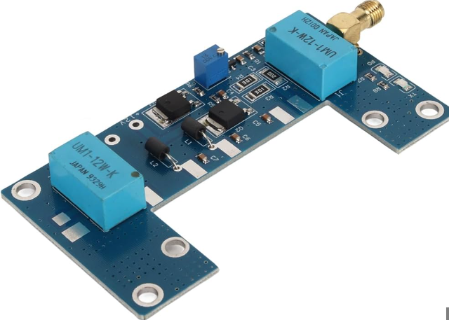
Designing printed circuit boards (PCBs) for optimal radio frequency (RF) power handling is a complex task that requires a deep understanding of both electrical engineering principles and practical design strategies.
The ability of a PCB to handle RF power efficiently is crucial in applications ranging from telecommunications to radar systems. To achieve this, several key factors must be considered, including material selection, trace design, thermal management, and impedance matching.
First and foremost, the choice of substrate material plays a pivotal role in RF power handling.
Materials with low dielectric loss and high thermal conductivity are preferred, as they minimize signal attenuation and effectively dissipate heat generated by high-power RF signals. Common materials include Rogers RO4000 series and Taconic RF-35, which offer excellent performance at high frequencies. The dielectric constant of the substrate should also be consistent to ensure signal integrity and minimize phase distortion.
In addition to material selection, the design of the PCB traces is critical.
Wider traces are generally better for RF power handling as they reduce the current density and, consequently, the resistive losses. However, the width of the traces must be balanced with the need to maintain controlled impedance. Microstrip and stripline configurations are commonly used to achieve this balance. Microstrip lines, which consist of a trace on the top layer of the PCB with a ground plane below, are easier to design and manufacture. Striplines, on the other hand, are sandwiched between two ground planes and offer better isolation and reduced radiation losses.
Thermal management is another essential aspect of optimizing RF power handling.
High-power RF signals generate significant heat, which can degrade the performance of the PCB and even cause physical damage if not properly managed. Effective thermal management strategies include the use of thermal vias, heat sinks, and thermal pads. Thermal vias are small holes filled with conductive material that connect the top and bottom layers of the PCB, allowing heat to dissipate more efficiently. Heat sinks and thermal pads can be attached to components that generate the most heat, further enhancing thermal dissipation.
Impedance matching is also crucial for efficient RF power handling.
Mismatched impedance can lead to signal reflections, which not only reduce the power delivered to the load but also increase the risk of damaging the RF components. To achieve proper impedance matching, designers often use techniques such as quarter-wave transformers, stub matching, and the use of matching networks composed of inductors and capacitors. Simulation tools like Advanced Design System (ADS) and High-Frequency Structure Simulator (HFSS) can be invaluable in optimizing impedance matching and ensuring that the PCB performs as intended.
Moreover, the layout of the PCB should be carefully planned to minimize parasitic effects and crosstalk between traces.
Keeping high-power RF traces away from sensitive analog or digital lines is essential to prevent interference. Ground planes should be continuous and unbroken to provide a stable reference point and reduce electromagnetic interference (EMI). Additionally, the use of guard traces and proper grounding techniques can further enhance the PCB’s ability to handle high RF power.
In conclusion, optimizing PCB RF power handling involves a multifaceted approach that includes careful material selection, trace design, thermal management, and impedance matching. By considering these factors and employing advanced simulation tools, designers can create PCBs that efficiently handle high-power RF signals, ensuring reliable performance in demanding applications.
Common Challenges in PCB RF Power Handling and How to Overcome Them
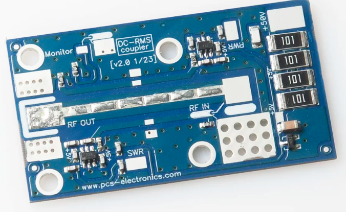
Printed Circuit Boards (PCBs) are integral to modern electronic devices, and their ability to handle Radio Frequency (RF) power is crucial for the performance of various applications, from telecommunications to medical devices. However, managing RF power on PCBs presents several challenges that engineers must address to ensure optimal functionality and reliability. Understanding these common challenges and the strategies to overcome them is essential for successful PCB design and implementation.
One of the primary challenges in PCB RF power handling is signal integrity.
High-frequency signals are susceptible to various forms of interference, including crosstalk, electromagnetic interference (EMI), and signal reflection. Crosstalk occurs when a signal transmitted on one trace induces an unwanted signal on an adjacent trace, leading to potential data corruption. To mitigate crosstalk, designers can increase the spacing between traces, use differential signaling, and implement ground planes to provide a return path for the signals, thereby reducing interference.
Electromagnetic interference is another significant concern.
EMI can originate from both external sources and internal components, potentially disrupting the RF signals on the PCB. Shielding techniques, such as using metal enclosures or incorporating ground planes, can help minimize EMI. Additionally, careful layout design, including the strategic placement of components and routing of traces, can reduce the susceptibility to EMI.
Signal reflection, caused by impedance mismatches, is another challenge that can degrade RF performance.
When the impedance of the transmission line does not match the load impedance, part of the signal is reflected back towards the source, causing signal distortion and loss. To address this issue, designers must ensure impedance matching by carefully selecting the width and spacing of traces, as well as using appropriate termination techniques, such as resistive or capacitive terminations.
Thermal management is also a critical aspect of PCB RF power handling.
High-power RF signals can generate significant heat, which, if not properly managed, can lead to component failure and reduced reliability. Effective thermal management strategies include using thermal vias to dissipate heat, incorporating heat sinks, and selecting materials with high thermal conductivity. Additionally, designers can optimize the layout to distribute heat more evenly across the PCB, preventing localized hotspots.
Material selection plays a vital role in RF power handling.
The dielectric properties of the PCB substrate material can significantly impact signal propagation and loss. Materials with low dielectric constant and low loss tangent are preferred for high-frequency applications, as they minimize signal attenuation and dispersion. Common materials used for RF PCBs include PTFE (Teflon), Rogers, and ceramic-filled laminates. Selecting the appropriate material based on the specific application requirements is crucial for achieving optimal performance.
Another challenge is the integration of passive components, such as capacitors and inductors, which are essential for RF circuits.
These components must be carefully selected and placed to ensure they do not introduce unwanted parasitic effects, such as inductance or capacitance, which can alter the circuit’s performance. Surface-mount technology (SMT) components are often preferred for RF applications due to their smaller size and lower parasitic effects compared to through-hole components.
In conclusion, PCB RF power handling involves addressing several challenges, including signal integrity, EMI, signal reflection, thermal management, material selection, and passive component integration. By employing strategies such as careful layout design, impedance matching, effective thermal management, and selecting appropriate materials and components, engineers can overcome these challenges and ensure the reliable performance of RF PCBs. Understanding and addressing these issues is essential for the successful design and implementation of high-frequency electronic devices.
Materials and Components for Enhanced PCB RF Power Handling
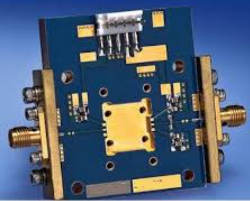
In the realm of high-frequency electronics, the ability of a printed circuit board (PCB) to handle radio frequency (RF) power is paramount. This capability hinges on the careful selection of materials and components, which collectively determine the efficiency, reliability, and performance of the PCB in RF applications. To begin with, the choice of substrate material is a critical factor.
Traditional FR-4 substrates, while cost-effective and widely used, often fall short in high-frequency applications due to their relatively high dielectric losses and inconsistent dielectric constant.
Instead, materials such as Rogers RO4000 series, Taconic, and PTFE-based laminates are preferred. These materials offer lower dielectric losses, stable dielectric constants, and better thermal management, which are essential for maintaining signal integrity and minimizing power loss.
Transitioning from substrate materials to conductive elements, the type of copper used in the PCB also plays a significant role.
High-frequency PCBs benefit from the use of low-profile or rolled copper, which has a smoother surface compared to standard electrodeposited copper. This smoothness reduces skin effect losses, a phenomenon where high-frequency currents tend to flow on the surface of conductors, thereby improving overall RF performance. Additionally, the thickness of the copper traces must be carefully considered. Thicker traces can handle higher currents and dissipate heat more effectively, but they also introduce parasitic inductance, which can adversely affect high-frequency signals. Therefore, a balance must be struck to optimize both power handling and signal integrity.
Moreover, the design and placement of components on the PCB are crucial for enhanced RF power handling.
Surface-mount components are generally preferred over through-hole components due to their lower parasitic inductance and capacitance. Furthermore, the layout should minimize the length of signal paths and avoid sharp bends, which can cause signal reflections and losses. Ground planes and power planes should be strategically placed to provide a low-impedance return path for RF currents, thereby reducing electromagnetic interference (EMI) and improving signal integrity.
Thermal management is another vital aspect that cannot be overlooked.
High RF power levels generate significant heat, which, if not properly managed, can degrade the performance and reliability of the PCB. Materials with high thermal conductivity, such as metal-core PCBs or those with thermal vias, can effectively dissipate heat away from critical components. Additionally, the use of thermal interface materials (TIMs) and heat sinks can further enhance thermal management, ensuring that the PCB operates within safe temperature limits.
In conjunction with material selection and thermal management, the use of advanced simulation tools can greatly aid in the design process.
Electromagnetic simulation software allows engineers to model and predict the behavior of RF signals within the PCB, identifying potential issues such as signal reflections, crosstalk, and impedance mismatches before physical prototypes are built. This proactive approach not only saves time and resources but also ensures that the final design meets the stringent requirements of high-frequency applications.
In conclusion, the ability of a PCB to handle RF power effectively is a multifaceted challenge that requires careful consideration of materials, components, and design practices. By selecting appropriate substrate materials, optimizing conductive elements, strategically placing components, managing thermal loads, and leveraging advanced simulation tools, engineers can design PCBs that excel in high-frequency environments. This holistic approach ensures that the PCB not only meets but exceeds the performance and reliability expectations in RF applications.


