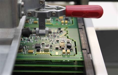
Via in pad pcb assembly
Benefits Of Using Via In Pad For High-Density PCB Designs
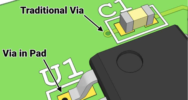
In the realm of high-density printed circuit board (PCB) designs, the implementation of via in pad technology has emerged as a pivotal advancement, offering a multitude of benefits that enhance both the performance and manufacturability of complex electronic assemblies. This technique, which involves placing vias directly beneath component pads, is particularly advantageous in scenarios where space constraints and signal integrity are paramount.
One of the primary benefits of using via in pad for high-density PCB designs is the significant reduction in board real estate.
As electronic devices continue to shrink in size while increasing in functionality, the demand for more compact and efficient PCB layouts has intensified. Via in pad technology addresses this challenge by allowing designers to place vias directly under the pads of surface-mounted components, thereby freeing up valuable space on the PCB. This space-saving attribute is crucial for accommodating the dense component placement required in modern electronic devices such as smartphones, tablets, and wearable technology.
Moreover, via in pad technology enhances signal integrity, which is a critical consideration in high-speed and high-frequency applications.
Traditional via placement can introduce unwanted inductance and capacitance, leading to signal degradation and potential performance issues. By integrating vias within the component pads, the signal path is shortened, and the associated parasitic effects are minimized. This results in improved signal transmission and reduced electromagnetic interference (EMI), ensuring that the PCB can operate reliably at higher frequencies.
In addition to space savings and improved signal integrity, via in pad technology also contributes to better thermal management.
Effective heat dissipation is essential for maintaining the reliability and longevity of electronic components, particularly in high-power applications. Vias placed within the pads can act as thermal vias, providing a direct path for heat to be conducted away from the component and into the PCB’s thermal plane. This efficient heat transfer mechanism helps to prevent overheating and ensures that the components operate within their specified temperature ranges.
Furthermore, via in pad technology can simplify the assembly process and enhance the overall manufacturability of high-density PCBs.
By reducing the need for additional routing and via placement, the complexity of the PCB layout is minimized, leading to more straightforward and cost-effective manufacturing processes. This simplification can also result in higher yields and reduced production times, as there are fewer opportunities for errors and defects during assembly.
However, it is important to acknowledge that the implementation of via in pad technology does come with certain challenges.
For instance, the process requires precise control over the via filling and plating to ensure reliable electrical connections and prevent solder wicking issues. Additionally, the cost of manufacturing PCBs with via in pad technology can be higher due to the specialized processes and materials involved. Despite these challenges, the benefits of via in pad technology often outweigh the drawbacks, particularly in high-density and high-performance applications where space, signal integrity, and thermal management are critical considerations.
In conclusion, via in pad technology offers a host of benefits for high-density PCB designs, including space savings, improved signal integrity, enhanced thermal management, and simplified assembly processes. As electronic devices continue to evolve and demand more compact and efficient PCB layouts, the adoption of via in pad technology is likely to become increasingly prevalent, driving further advancements in the field of PCB design and manufacturing.
Common Challenges And Solutions In Via In Pad PCB Assembly
Via in pad PCB assembly is a sophisticated technique used in modern electronics manufacturing to enhance the performance and reliability of printed circuit boards (PCBs). This method involves placing vias directly within the pads of surface-mounted components, which can significantly improve electrical performance and thermal management. However, despite its advantages, via in pad PCB assembly presents several challenges that manufacturers must address to ensure optimal functionality and reliability.
One of the primary challenges in via in pad PCB assembly is the potential for solder wicking.
When vias are placed within the pads, there is a risk that solder will flow into the via during the reflow process, leading to insufficient solder on the pad and poor solder joint formation. This can result in weak mechanical connections and unreliable electrical performance. To mitigate this issue, manufacturers often employ techniques such as via filling or plugging. Via filling involves filling the via with a conductive or non-conductive material before applying the solder mask, while via plugging uses a similar approach but with a different material. Both methods aim to prevent solder from wicking into the via, ensuring a robust solder joint.
Another significant challenge is the potential for voids in the solder joints.
Voids can occur when air or other gases become trapped in the solder during the reflow process. These voids can compromise the mechanical strength and thermal conductivity of the solder joint, leading to potential failures in the field. To address this issue, manufacturers can optimize their reflow profiles to ensure proper outgassing and minimize void formation. Additionally, using low-void solder pastes and implementing vacuum reflow processes can further reduce the occurrence of voids, enhancing the overall reliability of the assembly.
Thermal management is also a critical concern in via in pad PCB assembly.
The placement of vias within the pads can create thermal pathways that facilitate heat dissipation from high-power components. However, improper design or execution can lead to thermal imbalances, potentially causing overheating and damage to sensitive components. To overcome this challenge, careful thermal analysis and simulation are essential during the design phase. By strategically placing vias and optimizing the PCB layout, manufacturers can ensure efficient heat dissipation and maintain the thermal integrity of the assembly.
Furthermore, the mechanical stability of the PCB can be compromised if the vias are not properly designed and implemented.
Vias in pads can introduce stress concentrations, which may lead to cracking or delamination of the PCB material under mechanical or thermal cycling. To prevent such issues, manufacturers should adhere to industry standards and guidelines for via design, including appropriate via sizes, aspect ratios, and spacing. Additionally, using high-quality materials and advanced fabrication techniques can enhance the mechanical robustness of the PCB.
In conclusion, while via in pad PCB assembly offers numerous benefits in terms of electrical performance and thermal management, it also presents several challenges that must be carefully managed. By addressing issues such as solder wicking, void formation, thermal management, and mechanical stability, manufacturers can ensure the reliability and performance of their assemblies. Through meticulous design, process optimization, and adherence to industry best practices, the challenges associated with via in pad PCB assembly can be effectively mitigated, paving the way for the successful implementation of this advanced manufacturing technique.

Design Guidelines For Implementing Via In Pad In PCB Layouts
Implementing via in pad in PCB layouts is a sophisticated technique that can significantly enhance the performance and reliability of electronic circuits. This method involves placing vias directly within the component pads, which can offer numerous advantages, particularly in high-density and high-frequency applications. However, to fully leverage these benefits, it is crucial to adhere to specific design guidelines that ensure optimal functionality and manufacturability.
One of the primary considerations when implementing via in pad is the selection of appropriate materials.
The choice of substrate and copper thickness can impact the thermal and electrical performance of the PCB. For instance, high-frequency circuits often benefit from substrates with low dielectric constants and loss tangents. Additionally, the copper thickness should be chosen based on the current-carrying requirements and thermal management needs of the design. By carefully selecting these materials, designers can mitigate potential issues such as signal loss and overheating.
Another critical aspect is the via size and placement.
The diameter of the via should be minimized to reduce the impact on the pad’s mechanical integrity and solderability. However, it must still be large enough to ensure reliable electrical connections and effective heat dissipation. The placement of vias should also be strategically planned to avoid interference with other components and traces. This can be particularly challenging in high-density designs, where space is at a premium. Therefore, designers must balance the need for compact layouts with the requirements for reliable via placement.
Thermal management is another key factor in via in pad implementation.
Vias can serve as effective thermal conduits, helping to dissipate heat from critical components. To maximize this benefit, designers should consider using multiple vias in high-power areas. Additionally, the use of thermal vias can be complemented by other cooling strategies, such as heat sinks and thermal pads. By integrating these elements into the design, it is possible to maintain optimal operating temperatures and enhance the overall reliability of the PCB.
The soldering process also requires careful attention when using via in pad.
The presence of vias can lead to solder wicking, where the solder flows into the via and away from the pad, resulting in poor solder joints. To prevent this, designers can use techniques such as via tenting or plugging. Tenting involves covering the via with solder mask, while plugging fills the via with a non-conductive material. Both methods can effectively prevent solder wicking and ensure robust solder joints.
Furthermore, it is essential to consider the impact of via in pad on the PCB’s manufacturability.
While this technique offers numerous benefits, it can also introduce challenges in the fabrication process. For example, the additional steps required for via tenting or plugging can increase production time and costs. Therefore, designers should work closely with their PCB manufacturers to ensure that the design is feasible and cost-effective. By collaborating with manufacturers early in the design process, potential issues can be identified and addressed, leading to a smoother production cycle.
In conclusion, implementing via in pad in PCB layouts can offer significant advantages in terms of performance and reliability. However, it requires careful consideration of material selection, via size and placement, thermal management, soldering techniques, and manufacturability. By adhering to these design guidelines, designers can effectively leverage the benefits of via in pad while minimizing potential challenges. This approach not only enhances the functionality of the PCB but also ensures a reliable and cost-effective manufacturing process.
Cost Implications Of Via In Pad Technology In PCB Manufacturing
Via in pad technology, a method where vias are placed directly beneath surface mount pads, has become increasingly popular in printed circuit board (PCB) manufacturing due to its ability to save space and improve electrical performance. However, while this technology offers several advantages, it also comes with significant cost implications that manufacturers must carefully consider.
One of the primary cost drivers associated with via in pad technology is the complexity of the manufacturing process.
Unlike traditional vias, which are typically placed in non-critical areas of the PCB, via in pad requires precise placement and additional steps to ensure reliability. This often involves filling the vias with conductive or non-conductive materials and then planarizing the surface to create a smooth, even pad. These additional steps not only increase the time required for manufacturing but also necessitate specialized equipment and materials, thereby driving up costs.
Moreover, the materials used in via in pad technology can be more expensive than those used in traditional PCB manufacturing.
For instance, the conductive or non-conductive fill materials must meet stringent thermal and electrical performance criteria, which can add to the overall material costs. Additionally, the need for high-quality solder masks and surface finishes to ensure reliable soldering further contributes to the expense.
Another significant cost factor is the increased need for rigorous testing and quality control.
Via in pad technology is often used in high-density interconnect (HDI) PCBs, which are typically employed in advanced applications such as aerospace, medical devices, and high-performance computing. These applications demand the highest levels of reliability and performance, necessitating extensive testing and inspection processes. Advanced testing methods, such as X-ray inspection and automated optical inspection (AOI), are often required to detect potential issues like voids, misalignment, or insufficient fill, adding to the overall cost.
Furthermore, the design phase of PCBs utilizing via in pad technology can be more time-consuming and costly.
Engineers must carefully consider the placement of vias to avoid issues such as signal integrity problems and thermal management challenges. This often requires advanced design software and simulation tools, as well as additional design iterations, all of which contribute to higher design costs.
Despite these cost implications, the benefits of via in pad technology can often justify the investment, particularly for applications where space savings, improved electrical performance, and enhanced thermal management are critical. For example, in miniaturized devices such as smartphones and wearable technology, the ability to place vias directly beneath components can significantly reduce the overall footprint of the PCB, enabling more compact and efficient designs. Additionally, the improved electrical performance and reduced signal loss associated with via in pad technology can be crucial for high-speed and high-frequency applications.
In conclusion, while via in pad technology offers several advantages in terms of space savings and performance improvements, it also comes with significant cost implications. The increased complexity of the manufacturing process, the need for specialized materials, rigorous testing and quality control, and the more demanding design phase all contribute to higher costs. However, for applications where these benefits are critical, the investment in via in pad technology can be well worth the expense. Manufacturers must carefully weigh these cost factors against the potential advantages to determine the most appropriate approach for their specific needs.