Ttm pcb manufacturing
Trends In TTM PCB Manufacturing
TTM PCB manufacturing, a critical component in the electronics industry, has seen significant advancements and trends that are shaping its future. As technology continues to evolve, the demand for more sophisticated and reliable printed circuit boards (PCBs) has increased, driving innovation in manufacturing processes and materials.
One of the most notable trends in TTM PCB manufacturing is the shift towards miniaturization.
With the proliferation of portable electronic devices such as smartphones, tablets, and wearables, there is a growing need for smaller, yet highly efficient PCBs. This trend has led to the development of advanced manufacturing techniques such as high-density interconnect (HDI) technology, which allows for more components to be packed into a smaller area, thereby enhancing the functionality of the device without increasing its size.
In addition to miniaturization, there is a significant focus on improving the reliability and performance of PCBs.
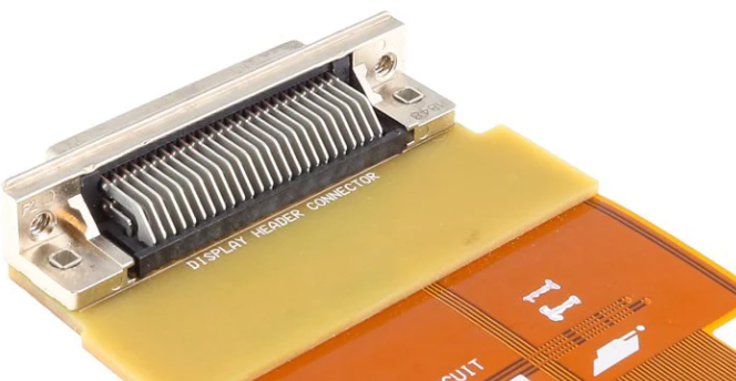
This has been achieved through the use of advanced materials and innovative manufacturing processes. For instance, the adoption of flexible PCBs, which can bend and twist without breaking, has opened up new possibilities for electronic device design. These flexible PCBs are particularly useful in applications where space is limited or where the PCB needs to conform to a specific shape. Moreover, the use of advanced materials such as high-temperature laminates and low-loss dielectrics has improved the thermal and electrical performance of PCBs, making them more suitable for high-speed and high-frequency applications.
Another important trend in TTM PCB manufacturing is the increasing emphasis on sustainability and environmental responsibility.
As the electronics industry faces growing scrutiny over its environmental impact, manufacturers are adopting greener practices and materials. This includes the use of lead-free solder, which reduces the environmental and health risks associated with lead, and the implementation of recycling programs to recover valuable materials from discarded PCBs. Additionally, manufacturers are investing in energy-efficient production processes and equipment to reduce their carbon footprint.
The integration of advanced technologies such as artificial intelligence (AI) and the Internet of Things (IoT) is also transforming TTM PCB manufacturing.
AI-powered design tools are enabling engineers to create more complex and optimized PCB layouts, while IoT-enabled manufacturing equipment allows for real-time monitoring and control of the production process. This not only improves the efficiency and accuracy of PCB manufacturing but also helps in identifying and addressing potential issues before they become critical, thereby reducing downtime and improving overall product quality.
Furthermore, the trend towards increased customization and rapid prototyping is gaining momentum in TTM PCB manufacturing.
With the rise of industries such as automotive, aerospace, and medical devices, there is a growing demand for custom PCBs that meet specific requirements. Advanced manufacturing techniques such as 3D printing and additive manufacturing are enabling manufacturers to produce highly customized PCBs quickly and cost-effectively. This has significantly reduced the time-to-market for new products and has allowed for greater flexibility in the design and production process.
In conclusion, the trends in TTM PCB manufacturing are being driven by the need for smaller, more reliable, and environmentally friendly PCBs, as well as the integration of advanced technologies and the demand for customization. As the electronics industry continues to evolve, TTM PCB manufacturers will need to stay at the forefront of these trends to remain competitive and meet the ever-changing needs of their customers. The future of TTM PCB manufacturing looks promising, with continued innovation and advancements paving the way for more efficient and sustainable production processes.
TTM PCB Manufacturing Process Overview
TTM PCB manufacturing is a complex and meticulous process that involves several stages, each critical to the production of high-quality printed circuit boards (PCBs). The journey begins with the design phase, where engineers create detailed schematics and layouts using advanced software tools. These designs are then converted into a format suitable for manufacturing, ensuring that every component and connection is accurately represented.
Once the design is finalized, the next step is to select the appropriate materials.
The choice of substrate, typically a fiberglass-reinforced epoxy laminate, is crucial as it affects the board’s performance and durability. Copper is then laminated onto the substrate to form the conductive pathways. This copper-clad laminate serves as the foundation for the subsequent processes.
The manufacturing process continues with the drilling stage, where precise holes are created to accommodate component leads and vias.
These holes are drilled using computer-controlled machines to ensure accuracy and consistency. Following drilling, the boards undergo a thorough cleaning process to remove any debris or contaminants that could interfere with the subsequent steps.
Next, the boards are subjected to a process known as electroless copper plating.
This involves depositing a thin layer of copper onto the drilled holes, creating a conductive path between the different layers of the PCB. This step is essential for establishing reliable electrical connections throughout the board.
After plating, the boards move on to the imaging stage.
Here, a photosensitive film is applied to the surface of the board, and the design is transferred onto the film using ultraviolet light. The exposed areas of the film are then developed, revealing the underlying copper that will form the circuit traces. This process is followed by an etching step, where the unwanted copper is removed, leaving behind the desired circuit pattern.
The next phase involves applying a solder mask, which is a protective layer that covers the circuit traces and prevents solder bridges during component assem bly.
The solder mask is typically applied using a screen-printing process and then cured using ultraviolet light. This step is crucial for ensuring the reliability and longevity of the PCB.
Following the application of the solder mask, the boards undergo a surface finish process.
This involves coating the exposed copper areas with a protective layer to prevent oxidation and improve solderability. Common surface finishes include hot air solder leveling (HASL), immersion gold, and organic solderability preservatives (OSP). Each finish has its advantages and is selected based on the specific requirements of the application.
The final stages of TTM PCB manufacturing involve the assembly and testing of the boards.
Components are placed onto the board using automated pick-and-place machines, and soldered in place using reflow or wave soldering techniques. Once assembled, the boards undergo rigorous testing to ensure they meet the required specifications and performance standards. This includes electrical testing, functional testing, and visual inspection to identify any defects or issues.
In conclusion, TTM PCB manufacturing is a highly detailed and precise process that requires careful attention to every stage, from design to final testing. Each step is critical to producing reliable and high-performance printed circuit boards that meet the stringent demands of modern electronic applications. By adhering to these meticulous processes, TTM ensures the delivery of top-quality PCBs that are essential for the success of various electronic devices and systems.

Benefits Of TTM PCB Manufacturing For High-Tech Industries
TTM PCB manufacturing has emerged as a pivotal process in the high-tech industries, offering a multitude of benefits that cater to the ever-evolving demands of modern technology. As the backbone of electronic devices, printed circuit boards (PCBs) are integral to the functionality and performance of a wide array of high-tech applications. The advantages of TTM PCB manufacturing are manifold, encompassing aspects such as precision, reliability, and scalability, which are crucial for industries that rely on cutting-edge technology.
One of the foremost benefits of TTM PCB manufacturing is its unparalleled precision.
High-tech industries, such as aerospace, medical devices, and telecommunications, require PCBs that meet stringent specifications and tolerances. TTM PCB manufacturing employs advanced techniques and state-of-the-art equipment to ensure that each PCB is produced with exacting accuracy. This level of precision is essential for the seamless operation of complex electronic systems, where even the slightest deviation can lead to significant malfunctions or failures.
In addition to precision, reliability is a cornerstone of TTM PCB manufacturing.
High-tech industries demand components that can withstand rigorous conditions and maintain consistent performance over extended periods. TTM PCB manufacturing processes incorporate rigorous quality control measures, including thorough testing and inspection at various stages of production. This ensures that the final product is not only reliable but also durable, capable of enduring the harsh environments often encountered in high-tech applications. Consequently, industries can trust that their electronic systems will function optimally, reducing the risk of costly downtime and repairs.
Scalability is another significant advantage offered by TTM PCB manufacturing.
As high-tech industries continue to grow and innovate, the need for scalable production solutions becomes increasingly important. TTM PCB manufacturing is designed to accommodate both small-scale prototypes and large-scale production runs, providing flexibility to meet the varying demands of different projects. This scalability is particularly beneficial for industries that require rapid prototyping and quick turnaround times, enabling them to bring new products to market faster and more efficiently.
Moreover, TTM PCB manufacturing supports the integration of advanced materials and technologies, which is essential for high-tech industries striving to stay ahead of the curve.
The ability to incorporate cutting-edge materials, such as high-frequency laminates and flexible substrates, allows for the development of PCBs that can support the latest technological advancements. This adaptability ensures that high-tech industries can continue to innovate and push the boundaries of what is possible, without being constrained by outdated manufacturing processes.
Furthermore, the environmental impact of manufacturing processes is an increasingly important consideration for high-tech industries.
TTM PCB manufacturing often incorporates eco-friendly practices, such as the use of lead-free solder and the implementation of waste reduction strategies. These practices not only help to minimize the environmental footprint of PCB production but also align with the growing emphasis on sustainability within the high-tech sector. By choosing TTM PCB manufacturing, industries can demonstrate their commitment to environmental responsibility while still achieving high-quality results.
In conclusion, the benefits of TTM PCB manufacturing for high-tech industries are extensive and multifaceted. The precision, reliability, scalability, and adaptability of this manufacturing process make it an ideal choice for industries that demand the highest standards of performance and innovation. As technology continues to advance at a rapid pace, TTM PCB manufacturing will undoubtedly play a crucial role in supporting the development and success of high-tech applications across various sectors.
Innovations In TTM PCB Manufacturing Techniques
The field of printed circuit board (PCB) manufacturing has witnessed significant advancements over the years, with TTM Technologies standing at the forefront of these innovations. As a leading global manufacturer, TTM has continually pushed the boundaries of PCB technology, integrating cutting-edge techniques to enhance performance, reliability, and efficiency.
One of the most notable innovations in TTM PCB manufacturing is the adoption of advanced materials.
Traditional PCBs primarily utilized FR-4, a composite material made of woven fiberglass cloth with an epoxy resin binder. However, TTM has incorporated high-frequency laminates and other advanced substrates to meet the demands of modern electronic applications. These materials offer superior thermal management, reduced signal loss, and enhanced mechanical stability, making them ideal for high-speed and high-frequency circuits.
In addition to material advancements, TTM has also revolutionized the manufacturing process through the implementation of laser direct imaging (LDI) technology.
LDI replaces traditional photolithography methods, which involve the use of photomasks and UV light to transfer circuit patterns onto the PCB substrate. By utilizing laser beams to directly image the circuit patterns, LDI offers higher precision and resolution, enabling the production of finer lines and spaces. This is particularly crucial for the miniaturization of electronic devices, where space constraints necessitate the use of smaller and more densely packed components.
Furthermore, TTM has embraced the concept of additive manufacturing, commonly known as 3D printing, in PCB production.
This technique allows for the creation of complex, multi-layered PCBs with intricate geometries that would be challenging to achieve using traditional subtractive methods. Additive manufacturing not only reduces material waste but also shortens production times, offering a more sustainable and efficient approach to PCB fabrication. The ability to rapidly prototype and iterate designs is another significant advantage, facilitating faster time-to-market for new electronic products.
Another key innovation in TTM PCB manufacturing is the integration of advanced inspection and testing methodologies.
Ensuring the quality and reliability of PCBs is paramount, given their critical role in electronic systems. TTM employs automated optical inspection (AOI) and automated X-ray inspection (AXI) technologies to detect defects and ensure the integrity of the PCBs. AOI uses high-resolution cameras to capture images of the PCB surface, while AXI provides a non-destructive means of inspecting internal layers and solder joints. These advanced inspection techniques enable early detection of potential issues, reducing the likelihood of failures in the final product.
Moreover, TTM has made significant strides in enhancing the environmental sustainability of its manufacturing processes.
The company has implemented various initiatives to minimize waste, reduce energy consumption, and lower the environmental impact of its operations. For instance, TTM has adopted water-based cleaning processes and lead-free soldering techniques, aligning with global environmental regulations and industry standards. Additionally, the company has invested in energy-efficient equipment and renewable energy sources to further reduce its carbon footprint.
In conclusion, TTM Technologies has consistently demonstrated its commitment to innovation in PCB manufacturing through the adoption of advanced materials, cutting-edge imaging and additive manufacturing techniques, rigorous inspection methodologies, and sustainable practices. These innovations not only enhance the performance and reliability of PCBs but also contribute to the overall advancement of the electronics industry. As technology continues to evolve, TTM remains poised to lead the way in developing next-generation PCB solutions that meet the ever-increasing demands of modern electronic applications.