Temspace- pcb assembly & soldering
Techniques For Efficient PCB Assembly
Efficient PCB assembly is a critical aspect of modern electronics manufacturing, requiring a blend of precision, expertise, and advanced technology. To achieve optimal results, several techniques must be employed, each contributing to the overall efficiency and reliability of the final product.
One of the foundational steps in PCB assembly is the preparation of the board and components.
This involves ensuring that the PCB is clean and free from contaminants, which can be achieved through various cleaning methods such as ultrasonic cleaning or using specialized solvents. Proper preparation sets the stage for successful component placement and soldering.
Moving forward, the application of solder paste is a crucial step that demands accuracy.
Solder paste is typically applied using a stencil, which ensures that the paste is deposited only on the pads where components will be placed. The thickness and consistency of the solder paste must be carefully controlled to avoid issues such as bridging or insufficient solder joints. Automated solder paste printers are often used in high-volume production to maintain consistency and precision.
Once the solder paste is applied, the next step is component placement.
This process can be performed manually or through automated pick-and-place machines. Automated systems are preferred for their speed and accuracy, especially in high-volume production environments. These machines use vision systems to ensure that components are placed correctly, minimizing the risk of misalignment or incorrect orientation. Proper component placement is essential for ensuring reliable electrical connections and overall functionality of the PCB.
Following component placement, the soldering process begins.
Reflow soldering is the most common method used in PCB assembly, particularly for surface-mount technology (SMT) components. During reflow soldering, the assembled PCB is passed through a reflow oven where it is subjected to controlled temperature profiles. The solder paste melts and forms solid solder joints as the board cools down. It is imperative to monitor the temperature profile closely to prevent defects such as cold solder joints or thermal damage to components.
In addition to reflow soldering, wave soldering is another technique used, primarily for through-hole components.
In wave soldering, the PCB is passed over a wave of molten solder, which ensures that all through-hole connections are soldered simultaneously. This method is efficient for boards with a high density of through-hole components but requires careful control of solder temperature and wave height to avoid defects.
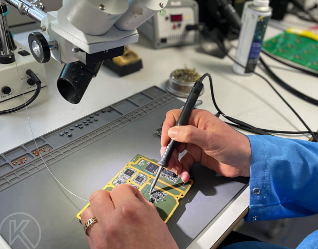
Post-soldering inspection is a vital step to ensure the quality and reliability of the assembled PCB.
Automated optical inspection (AOI) systems are commonly used to detect soldering defects, component misplacements, and other anomalies. AOI systems use high-resolution cameras and advanced algorithms to compare the assembled board against a predefined standard, allowing for quick identification and correction of issues.
Finally, functional testing is conducted to verify that the assembled PCB performs as intended. This may involve in-circuit testing (ICT), where electrical probes are used to test individual components and connections, or functional testing, where the board is tested under operating conditions. Ensuring that the PCB functions correctly before it is integrated into the final product is crucial for maintaining quality and reliability.
In conclusion, efficient PCB assembly requires meticulous attention to detail at every stage, from preparation and solder paste application to component placement, soldering, inspection, and testing. By employing advanced techniques and technologies, manufacturers can achieve high-quality, reliable PCBs that meet the demands of modern electronic devices.
Common Soldering Mistakes And How To Avoid Them
Soldering is a critical process in PCB assembly, requiring precision and attention to detail to ensure the functionality and reliability of electronic devices. However, even experienced technicians can fall prey to common soldering mistakes that can compromise the integrity of the final product. Understanding these pitfalls and learning how to avoid them is essential for anyone involved in PCB assembly and soldering.
One prevalent mistake is the use of insufficient heat.
When the soldering iron is not hot enough, the solder may not flow properly, leading to weak joints that can easily break under stress. To avoid this, it is crucial to ensure that the soldering iron is adequately preheated to the recommended temperature for the specific type of solder being used. Additionally, maintaining a clean and well-tinned soldering iron tip can facilitate better heat transfer, resulting in stronger and more reliable solder joints.
Conversely, excessive heat can also pose significant problems.
Overheating can damage the PCB and its components, leading to delamination, lifted pads, or even complete component failure. To mitigate this risk, it is important to use a temperature-controlled soldering station and to apply heat for only as long as necessary to achieve a good solder joint. Practicing proper technique, such as using the correct tip size and shape for the task at hand, can also help in managing heat application effectively.
Another common issue is the use of too much or too little solder.
Excessive solder can create bridges between adjacent pads or leads, causing short circuits and potential device failure. On the other hand, insufficient solder can result in weak joints that may not provide adequate electrical connectivity. To strike the right balance, it is essential to apply just enough solder to form a smooth, shiny, and concave fillet around the joint. Using flux can also aid in achieving better solder flow and adhesion, reducing the likelihood of these issues.
Cold solder joints are another frequent problem, often caused by moving the components before the solder has fully solidified.
These joints appear dull and grainy and can lead to intermittent connections or complete circuit failure. To prevent cold solder joints, it is important to hold the components steady until the solder has cooled and solidified completely. Using a third hand tool or a PCB holder can provide the necessary stability during the soldering process.
Furthermore, improper cleaning of the PCB and components before soldering can lead to poor solder adhesion and unreliable connections.
Contaminants such as oils, dust, and oxidation can prevent the solder from bonding properly with the surfaces. To avoid this, it is essential to clean the PCB and components thoroughly using isopropyl alcohol or a specialized PCB cleaner before beginning the soldering process. Ensuring a clean working environment can also help in minimizing the introduction of contaminants.
Lastly, neglecting to inspect and test the solder joints can result in undetected issues that may cause device failure down the line.
Visual inspection under magnification can help identify problems such as cold joints, solder bridges, and insufficient solder. Additionally, performing electrical tests, such as continuity checks and functional testing, can verify the integrity of the solder joints and the overall functionality of the assembled PCB.
In conclusion, avoiding common soldering mistakes requires a combination of proper technique, appropriate tools, and diligent inspection. By understanding the potential pitfalls and implementing best practices, technicians can ensure the production of high-quality, reliable PCBs that meet the stringent demands of modern electronic devices.

The Importance Of Quality Control In PCB Soldering
In the realm of electronics manufacturing, the significance of quality control in printed circuit board (PCB) soldering cannot be overstated. As the backbone of virtually all electronic devices, PCBs require meticulous attention to detail during assembly and soldering to ensure functionality, reliability, and longevity. Quality control processes are integral to achieving these objectives, as they help identify and rectify potential issues before they escalate into costly failures.
To begin with, quality control in PCB soldering involves a series of systematic checks and balances designed to maintain high standards throughout the manufacturing process.
This includes inspecting the raw materials, such as the PCB substrates and soldering components, to ensure they meet specified criteria. By verifying the quality of these materials at the outset, manufacturers can prevent defects that might arise from substandard inputs. Furthermore, the precision of the soldering process itself is critical. Automated soldering machines, such as reflow ovens and wave soldering systems, must be calibrated and maintained regularly to ensure consistent performance. Any deviation in temperature profiles or solder paste application can lead to issues such as cold solder joints, bridging, or insufficient wetting, all of which can compromise the integrity of the final product.
Moreover, human oversight remains a crucial element of quality control in PCB soldering.
Skilled technicians are often required to perform visual inspections and manual touch-ups, particularly for complex or high-density boards where automated systems may fall short. These professionals are trained to identify subtle defects that machines might overlook, such as micro-cracks or incomplete solder joints. Their expertise ensures that even the most minute imperfections are addressed, thereby enhancing the overall reliability of the PCB.
In addition to visual inspections, advanced testing methods play a pivotal role in quality control.
Techniques such as X-ray inspection, automated optical inspection (AOI), and in-circuit testing (ICT) provide a deeper level of scrutiny, allowing manufacturers to detect hidden defects that are not visible to the naked eye. For instance, X-ray inspection can reveal voids or misalignments within solder joints, while AOI systems use high-resolution cameras to compare the assembled board against a predefined standard. ICT, on the other hand, involves applying electrical signals to the PCB to verify the functionality of individual components and connections. These testing methods collectively contribute to a comprehensive quality control strategy, ensuring that each PCB meets the required specifications before it reaches the end user.
Furthermore, the importance of quality control in PCB soldering extends beyond the manufacturing floor.
It has significant implications for the end product’s performance and the manufacturer’s reputation. A single defective PCB can lead to the failure of an entire electronic device, resulting in customer dissatisfaction, warranty claims, and potential recalls. By implementing rigorous quality control measures, manufacturers can mitigate these risks, thereby safeguarding their brand image and customer trust.
In conclusion, quality control in PCB soldering is a multifaceted process that encompasses material inspection, precise soldering techniques, human oversight, and advanced testing methods. Each of these elements plays a vital role in ensuring the production of high-quality PCBs that meet stringent industry standards. As electronic devices continue to evolve and become more sophisticated, the need for robust quality control measures in PCB soldering will only grow more critical. By prioritizing quality at every stage of the manufacturing process, companies can deliver reliable and durable products that stand the test of time.
Innovations In PCB Assembly Technology
Printed Circuit Board (PCB) assembly and soldering have undergone significant advancements in recent years, driven by the relentless pursuit of efficiency, precision, and reliability in electronic manufacturing. These innovations are not only enhancing the quality of electronic devices but also streamlining production processes, thereby reducing costs and time-to-market.
One of the most notable advancements in PCB assembly technology is the development of Surface Mount Technology (SMT).
SMT has revolutionized the way components are mounted on PCBs, allowing for smaller, lighter, and more complex designs. Unlike traditional through-hole technology, which requires drilling holes into the PCB, SMT components are placed directly onto the surface of the board. This method not only saves space but also improves electrical performance and reliability.
In addition to SMT, the advent of automated assembly machines has significantly improved the speed and accuracy of PCB assembly.
These machines, equipped with advanced vision systems and precision placement capabilities, can place thousands of components per hour with remarkable accuracy. This automation reduces the likelihood of human error, ensuring consistent quality across large production runs. Furthermore, the integration of machine learning algorithms into these systems allows for real-time monitoring and adjustment, further enhancing the efficiency and reliability of the assembly process.
Another critical innovation in PCB assembly is the use of advanced soldering techniques.
Traditional wave soldering, while still in use, is being increasingly supplemented by reflow soldering and selective soldering methods. Reflow soldering, in particular, has become the standard for SMT components. This process involves applying solder paste to the PCB, placing the components, and then heating the assembly in a reflow oven. The controlled heating process ensures that the solder melts and forms reliable connections without damaging the components or the PCB itself. Selective soldering, on the other hand, is used for through-hole components and involves precisely applying solder only to the required areas, minimizing the risk of thermal damage and improving overall solder joint quality.
Moreover, the introduction of lead-free soldering has been a significant step forward in making PCB assembly more environmentally friendly.
Lead-free solders, typically composed of tin, silver, and copper, offer comparable performance to traditional lead-based solders while eliminating the health and environmental risks associated with lead. The transition to lead-free soldering has been driven by stringent regulations, such as the Restriction of Hazardous Substances (RoHS) directive, which mandates the reduction of hazardous materials in electronic products.
The use of advanced materials and coatings in PCB assembly has also contributed to improved performance and durability.
High-temperature laminates, for instance, allow PCBs to withstand the rigors of modern electronic applications, including those in automotive and aerospace industries. Additionally, conformal coatings protect the assembled PCBs from environmental factors such as moisture, dust, and chemicals, thereby extending the lifespan of electronic devices.
In conclusion, the innovations in PCB assembly and soldering technology are transforming the electronics manufacturing landscape.
From the adoption of Surface Mount Technology and automated assembly machines to advanced soldering techniques and environmentally friendly materials, these advancements are driving improvements in efficiency, precision, and reliability. As the demand for more sophisticated and compact electronic devices continues to grow, the ongoing evolution of PCB assembly technology will undoubtedly play a crucial role in meeting these challenges and shaping the future of electronics manufacturing.