Single sided flex pcb
Advantages Of Single Sided Flex PCBs In Modern Electronics
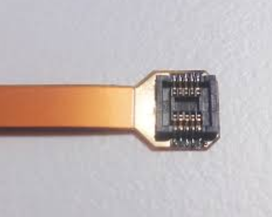
Single-sided flexible printed circuit boards (PCBs) have become increasingly prominent in modern electronics due to their unique advantages. These PCBs consist of a single conductive layer of metal, typically copper, on a flexible substrate, which allows for a range of applications that traditional rigid PCBs cannot accommodate.
One of the primary benefits of single-sided flex PCBs is their ability to conform to various shapes and contours, making them ideal for use in compact and complex electronic devices where space is at a premium.
In addition to their flexibility, single-sided flex PCBs offer significant weight reduction compared to their rigid counterparts.
This is particularly advantageous in industries such as aerospace, automotive, and consumer electronics, where minimizing weight is crucial for performance and efficiency. The lightweight nature of these PCBs contributes to the overall reduction in the weight of the final product, thereby enhancing its portability and ease of use.
Moreover, single-sided flex PCBs provide excellent reliability and durability.
The flexible substrate material, often made from polyimide or polyester, is resistant to high temperatures and harsh environmental conditions. This makes these PCBs suitable for applications that require long-term stability and performance under challenging conditions. For instance, in the automotive industry, single-sided flex PCBs are used in various sensors and control systems that must withstand extreme temperatures and vibrations.
Another notable advantage of single-sided flex PCBs is their cost-effectiveness.
The manufacturing process for these PCBs is relatively straightforward, involving fewer steps and materials compared to multi-layer or rigid PCBs. This simplicity translates to lower production costs, making single-sided flex PCBs an economical choice for many electronic applications. Additionally, the reduced need for connectors and interconnects in flexible circuits further decreases assembly costs and enhances overall system reliability.
The design versatility of single-sided flex PCBs also cannot be overlooked.
Engineers can create intricate and compact designs that would be impossible with rigid PCBs. This flexibility in design allows for innovative product development, enabling the creation of smaller, lighter, and more efficient electronic devices. For example, in the medical field, single-sided flex PCBs are used in wearable health monitoring devices that require a high degree of flexibility and miniaturization.
Furthermore, single-sided flex PCBs contribute to improved signal integrity and reduced electromagnetic interference (EMI).
The close proximity of the conductive traces on a single layer minimizes the potential for signal loss and crosstalk, ensuring reliable performance in high-frequency applications. This characteristic is particularly beneficial in telecommunications and data transmission devices, where maintaining signal integrity is paramount.
In conclusion, the advantages of single-sided flex PCBs in modern electronics are manifold. Their flexibility, lightweight nature, reliability, cost-effectiveness, design versatility, and improved signal integrity make them an indispensable component in a wide range of applications. As technology continues to advance and the demand for smaller, more efficient electronic devices grows, the role of single-sided flex PCBs is likely to become even more significant. Their ability to meet the stringent requirements of various industries while offering practical and economic benefits underscores their importance in the ever-evolving landscape of modern electronics.

Design Tips For Single Sided Flex PCBs
Designing single-sided flexible printed circuit boards (PCBs) requires a meticulous approach to ensure optimal performance and reliability. These PCBs, known for their flexibility and lightweight properties, are increasingly used in various applications, from consumer electronics to medical devices. To achieve a successful design, several key considerations must be taken into account.
Firstly, material selection is paramount.
The choice of substrate material significantly impacts the flexibility, durability, and overall performance of the PCB.
Polyimide is a popular choice due to its excellent thermal stability and mechanical properties. It is crucial to select a material that can withstand the environmental conditions the PCB will be exposed to, including temperature variations and mechanical stress.
Next, the layout design must be carefully planned.
Since single-sided flex PCBs have conductive traces on only one side, efficient use of space is essential. Designers should aim to minimize the length of the traces to reduce resistance and potential signal loss. Additionally, placing components strategically can help in maintaining the board’s flexibility. For instance, heavier components should be placed near the edges or in areas that are less likely to bend.
Transitioning to the aspect of trace routing, it is important to maintain a consistent trace width and spacing.
This consistency helps in preventing issues such as signal interference and crosstalk. Moreover, using curved traces instead of sharp angles can enhance the board’s flexibility and reduce stress concentrations that could lead to cracking or failure. It is also advisable to avoid placing vias in areas that will experience significant bending, as this can compromise the integrity of the connections.
Thermal management is another critical factor in the design of single-sided flex PCBs.
Since these boards are often used in compact and high-density applications, effective heat dissipation is necessary to prevent overheating. Incorporating thermal reliefs and using materials with good thermal conductivity can help manage heat distribution. Additionally, designers should consider the placement of heat-generating components and ensure there is adequate spacing to allow for proper airflow.
Furthermore, the choice of adhesive and coverlay materials plays a significant role in the overall performance of the PCB.
The adhesive must provide strong bonding without compromising flexibility. Similarly, the coverlay, which protects the conductive traces, should be durable and capable of withstanding the operational environment. It is essential to select materials that are compatible with the substrate and can endure the mechanical and thermal stresses encountered during use.
In addition to these considerations, testing and validation are crucial steps in the design process.
Prototyping and rigorous testing can help identify potential issues early on, allowing for necessary adjustments before mass production. Flexural testing, in particular, is important to ensure the PCB can withstand repeated bending and flexing without failure.
Finally, collaboration with experienced manufacturers can greatly enhance the design process.
Manufacturers with expertise in flexible PCBs can provide valuable insights and recommendations, helping to optimize the design for manufacturability and performance. They can also assist in selecting appropriate materials and ensuring compliance with industry standards.
In conclusion, designing single-sided flex PCBs involves a comprehensive approach that encompasses material selection, layout planning, trace routing, thermal management, and thorough testing. By carefully considering these factors and leveraging the expertise of experienced manufacturers, designers can create reliable and high-performing flexible PCBs suitable for a wide range of applications.

Common Applications Of Single Sided Flex PCBs
Single-sided flexible printed circuit boards (PCBs) have become an integral component in various industries due to their unique properties and advantages. These PCBs consist of a single conductive layer of metal, typically copper, which is laminated onto a flexible dielectric film. This construction allows for a high degree of flexibility, making them suitable for applications where space constraints and mechanical stress are significant considerations. As we delve into the common applications of single-sided flex PCBs, it becomes evident that their versatility and adaptability are key factors driving their widespread adoption.
One of the primary applications of single-sided flex PCBs is in the consumer electronics industry.
Devices such as smartphones, tablets, and wearable technology often require compact and lightweight components to maintain their sleek designs and portability. Single-sided flex PCBs are ideal for these devices because they can be bent and folded to fit into tight spaces without compromising their electrical performance. Additionally, their ability to withstand repeated flexing makes them suitable for use in devices with moving parts, such as foldable smartphones and smartwatches.
Transitioning to the automotive industry, single-sided flex PCBs play a crucial role in modern vehicle design.
As vehicles become more technologically advanced, the demand for reliable and efficient electronic systems has increased. Single-sided flex PCBs are used in various automotive applications, including dashboard displays, infotainment systems, and advanced driver-assistance systems (ADAS). Their flexibility allows for easy integration into the complex and often confined spaces within a vehicle’s interior. Moreover, their durability ensures that they can withstand the harsh conditions typically encountered in automotive environments, such as extreme temperatures and vibrations.
In the medical field, single-sided flex PCBs are utilized in a wide range of diagnostic and therapeutic devices.
Medical equipment often requires precise and reliable electronic components to ensure accurate performance. Single-sided flex PCBs are found in devices such as hearing aids, pacemakers, and portable diagnostic tools. Their flexibility and lightweight nature make them particularly suitable for wearable medical devices, which need to be comfortable for the patient while providing consistent functionality. Furthermore, the biocompatibility of certain flexible materials used in these PCBs ensures that they can be safely used in direct contact with the human body.
The aerospace and defense sectors also benefit from the unique properties of single-sided flex PCBs.
In these industries, the need for lightweight and reliable components is paramount due to the stringent weight and space limitations of aircraft and defense equipment. Single-sided flex PCBs are employed in various applications, including communication systems, navigation equipment, and control systems. Their ability to endure extreme environmental conditions, such as high altitudes and rapid temperature changes, makes them an excellent choice for aerospace and defense applications.
Lastly, the industrial sector leverages single-sided flex PCBs in numerous applications, ranging from robotics to industrial automation systems. In these settings, the flexibility and durability of single-sided flex PCBs enable them to be used in dynamic and demanding environments. For instance, in robotic arms, these PCBs can be integrated into joints and moving parts, allowing for seamless operation without the risk of damage due to repeated motion. Additionally, their resistance to chemicals and other harsh substances commonly found in industrial environments ensures long-term reliability and performance.
In conclusion, single-sided flex PCBs are indispensable in a variety of industries due to their flexibility, durability, and adaptability. From consumer electronics to automotive, medical, aerospace, defense, and industrial applications, these PCBs provide innovative solutions to complex design challenges, enabling the development of advanced and reliable electronic systems.

Manufacturing Process Of Single Sided Flex PCBs
The manufacturing process of single-sided flexible printed circuit boards (PCBs) involves a series of meticulously coordinated steps, each contributing to the creation of a highly reliable and efficient electronic component. Single-sided flex PCBs, characterized by their ability to bend and flex without breaking, are widely used in various applications, including wearable electronics, medical devices, and consumer gadgets. Understanding the manufacturing process of these versatile components is essential for appreciating their complexity and functionality.
To begin with, the process starts with the selection of the base material, typically a flexible substrate such as polyimide or polyester.
These materials are chosen for their excellent thermal stability, mechanical strength, and flexibility. The substrate is then coated with a thin layer of copper, which serves as the conductive material for the circuit. This copper layer is usually applied through a process called lamination, where the copper foil is bonded to the substrate under heat and pressure.
Following the lamination, the next step is to create the circuit pattern on the copper layer.
This is achieved through a process known as photolithography. Initially, a photosensitive resist material is applied to the copper surface. The resist-coated substrate is then exposed to ultraviolet (UV) light through a photomask, which contains the desired circuit pattern. The areas of the resist exposed to the UV light harden, while the unexposed areas remain soft and can be washed away using a developer solution. This leaves behind a precise pattern of resist on the copper layer.
Subsequently, the exposed copper areas are etched away using a chemical etchant, typically a solution of ferric chloride or ammonium persulfate.
The resist protects the desired circuit pattern during this etching process, ensuring that only the unwanted copper is removed. After etching, the remaining resist is stripped away, revealing the copper circuit pattern on the flexible substrate.
The next phase involves drilling holes, known as vias, into the substrate if required. These vias are used to create electrical connections between different layers of the PCB or to mount components. In single-sided flex PCBs, vias are less common but may still be necessary for certain designs. The drilling can be performed using mechanical drills or laser technology, depending on the precision required.
Once the vias are drilled, the PCB undergoes a cleaning process to remove any debris or contaminants.
This is crucial for ensuring the reliability and performance of the final product. The cleaned PCB is then subjected to a surface treatment, such as electroless nickel immersion gold (ENIG) or hot air solder leveling (HASL), to enhance solderability and protect the copper from oxidation.
The final steps in the manufacturing process involve the application of a protective solder mask and the addition of silkscreen markings.
The solder mask, typically a green or other colored epoxy, is applied over the entire surface of the PCB except for the pads where components will be soldered. This mask prevents solder bridges and short circuits during assembly. The silkscreen markings, applied using a screen-printing process, provide important information such as component labels and reference designators.
In conclusion, the manufacturing process of single-sided flex PCBs is a complex and precise series of steps that transform raw materials into highly functional electronic components. Each stage, from material selection and lamination to photolithography, etching, drilling, and surface treatment, plays a critical role in ensuring the quality and performance of the final product. By understanding this process, one can better appreciate the intricate engineering and craftsmanship involved in creating these versatile and essential components.


