Rs pcb assembly
Revolutionizing Electronics: The Future of RS PCB Assembly
The field of electronics has witnessed remarkable advancements over the past few decades, and one of the pivotal elements driving this progress is the evolution of printed circuit board (PCB) assembly.
Among the various methodologies, RS PCB assembly has emerged as a revolutionary approach, significantly enhancing the efficiency, reliability, and scalability of electronic devices. This article delves into the transformative impact of RS PCB assembly on the electronics industry, exploring its benefits, technological innovations, and future prospects.
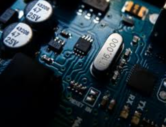
To begin with, RS PCB assembly, or Reflow Soldering PCB assembly, is a process that involves the precise placement of electronic components onto a PCB, followed by the application of solder paste and subsequent heating to create robust electrical connections.
This method has gained widespread adoption due to its ability to accommodate complex and densely packed circuit designs, which are increasingly common in modern electronic devices.
The precision and reliability of RS PCB assembly have made it indispensable in the production of smartphones, computers, medical devices, and a myriad of other high-tech products.
One of the primary advantages of RS PCB assembly is its efficiency.
Traditional soldering techniques often require manual intervention, which can be time-consuming and prone to human error. In contrast, RS PCB assembly leverages automated machinery and advanced software to streamline the entire process. This automation not only accelerates production but also ensures consistent quality across large volumes of PCBs. Consequently, manufacturers can meet the growing demand for electronic devices without compromising on performance or reliability.
Moreover, RS PCB assembly has significantly improved the reliability of electronic devices.
The reflow soldering process creates strong and durable solder joints, which are less susceptible to mechanical stress and thermal cycling. This enhanced reliability is particularly crucial in applications where electronic devices are subjected to harsh environments or continuous operation. For instance, in the automotive and aerospace industries, where safety and durability are paramount, RS PCB assembly has become the standard practice.
In addition to efficiency and reliability, RS PCB assembly has also facilitated the miniaturization of electronic devices.
As consumer preferences shift towards smaller, more portable gadgets, the ability to pack more functionality into compact form factors has become a competitive advantage. RS PCB assembly supports the integration of surface-mount technology (SMT) components, which are smaller and lighter than their through-hole counterparts. This capability has enabled the development of sleek and lightweight devices without sacrificing performance.
Technological innovations continue to push the boundaries of RS PCB assembly.
Advances in materials science have led to the development of high-performance solder pastes and fluxes, which enhance the quality of solder joints and reduce defects. Additionally, the integration of artificial intelligence and machine learning into assembly processes has enabled real-time monitoring and optimization, further improving yield rates and reducing waste. These innovations are paving the way for even more sophisticated and reliable electronic devices in the future.
Looking ahead, the future of RS PCB assembly appears promising.
As the Internet of Things (IoT) and 5G technologies gain traction, the demand for advanced PCBs is expected to surge. RS PCB assembly, with its proven track record of efficiency, reliability, and scalability, is well-positioned to meet this demand. Furthermore, ongoing research and development efforts are likely to yield new techniques and materials that will further enhance the capabilities of RS PCB assembly.
In conclusion, RS PCB assembly has revolutionized the electronics industry by providing a highly efficient, reliable, and scalable method for producing advanced PCBs. Its impact is evident in the proliferation of sophisticated electronic devices that have become integral to modern life. As technological innovations continue to emerge, RS PCB assembly will undoubtedly play a crucial role in shaping the future of electronics, driving further advancements and enabling new possibilities.
Step-by-Step Guide to RS PCB Assembly for Beginners
Printed Circuit Board (PCB) assembly is a critical process in the manufacturing of electronic devices, and understanding the steps involved is essential for beginners. RS PCB assembly, in particular, refers to the assembly of PCBs using components sourced from RS Components, a leading distributor of electronic, electrical, and industrial products. This guide aims to provide a comprehensive overview of the step-by-step process involved in RS PCB assembly, ensuring that even those new to the field can grasp the fundamental concepts and procedures.
To begin with, the initial step in RS PCB assembly is the design phase.
During this stage, engineers use specialized software to create a schematic diagram of the circuit. This diagram serves as a blueprint, detailing the placement of components and the connections between them. Once the schematic is complete, it is converted into a layout design, which specifies the physical arrangement of components on the PCB. This layout is then used to generate Gerber files, which are essential for the subsequent manufacturing process.
Following the design phase, the next step is the procurement of components.
RS Components offers a wide range of electronic parts, making it a convenient source for all necessary materials. It is crucial to ensure that all components meet the required specifications and are compatible with the design. Once the components are procured, they are inspected for quality and accuracy to prevent any issues during assembly.
The third step involves the preparation of the PCB itself.
This includes cleaning the board to remove any contaminants that could affect the soldering process. Additionally, a solder mask is applied to protect the board and ensure that solder only adheres to the designated areas. The application of a silkscreen layer follows, which provides labels and markings to assist in the placement of components.
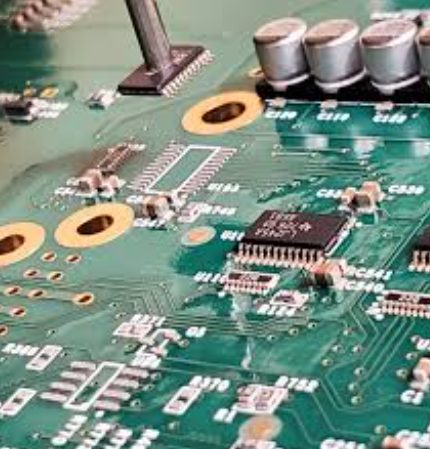
Subsequently, the assembly process begins with the placement of components on the PCB.
This can be done manually or using automated machines, depending on the complexity and volume of the production. Surface Mount Technology (SMT) is commonly used for placing components on the surface of the board, while Through-Hole Technology (THT) involves inserting component leads into holes drilled in the PCB. Both methods require precision to ensure that components are correctly aligned and securely attached.
Once the components are in place, the next step is soldering.
Soldering involves melting a metal alloy to create a strong electrical connection between the components and the PCB. For SMT components, reflow soldering is typically used, where the board is passed through an oven to melt the solder paste. For THT components, wave soldering or hand soldering may be employed. It is essential to inspect the solder joints for any defects, such as cold solder joints or bridges, which could compromise the functionality of the PCB.
After soldering, the assembled PCB undergoes a series of tests to verify its performance.
These tests include visual inspection, automated optical inspection (AOI), and functional testing. Any defects identified during testing are addressed through rework or repair processes. Finally, the PCB is cleaned to remove any residual flux or contaminants, ensuring that it meets the required standards for quality and reliability.
In conclusion, RS PCB assembly involves a meticulous process that begins with design and component procurement, followed by board preparation, component placement, soldering, and testing. By understanding each step and ensuring attention to detail, beginners can successfully navigate the complexities of PCB assembly and contribute to the production of high-quality electronic devices.
Top 5 Challenges in RS PCB Assembly and How to Overcome Them
RS PCB assembly, or Radio Signal Printed Circuit Board assembly, is a critical process in the manufacturing of electronic devices that rely on radio frequency (RF) communication. This intricate procedure involves several challenges that can impact the performance and reliability of the final product. Understanding these challenges and implementing effective strategies to overcome them is essential for ensuring high-quality RS PCB assemblies.
One of the foremost challenges in RS PCB assembly is signal integrity.
Maintaining signal integrity is crucial because any degradation can lead to poor performance or complete failure of the device. Signal integrity issues often arise from improper layout design, such as inadequate spacing between traces or incorrect impedance matching. To mitigate these issues, it is essential to follow best practices in PCB design, including maintaining consistent trace widths, using controlled impedance traces, and ensuring proper grounding. Additionally, employing simulation tools during the design phase can help identify potential signal integrity problems before they become critical.
Another significant challenge is thermal management. RS PCBs often operate at high frequencies, which can generate substantial heat.
Excessive heat can damage components and degrade the performance of the PCB. Effective thermal management involves using materials with high thermal conductivity, such as copper, and incorporating thermal vias to dissipate heat. Moreover, designing the PCB with adequate spacing between heat-generating components and using heat sinks or thermal pads can further enhance heat dissipation. Implementing these strategies can help maintain the optimal operating temperature of the RS PCB, thereby ensuring its longevity and reliability.
Component placement accuracy is also a critical factor in RS PCB assembly.
The precise placement of components is essential to avoid issues such as misalignment, which can lead to poor solder joints and connectivity problems. Automated pick-and-place machines are commonly used to achieve high placement accuracy. However, it is equally important to ensure that the components are correctly oriented and that the machine is properly calibrated. Regular maintenance and calibration of the pick-and-place equipment can significantly reduce placement errors and improve the overall quality of the assembly.
Furthermore, soldering quality is a vital aspect of RS PCB assembly.
Poor soldering can result in weak joints, which can cause intermittent connections or complete circuit failure. To overcome this challenge, it is crucial to use high-quality soldering materials and to follow proper soldering techniques. Employing automated soldering processes, such as reflow soldering, can ensure consistent and reliable solder joints. Additionally, conducting thorough inspections using X-ray or automated optical inspection (AOI) systems can help identify and rectify soldering defects before the final assembly.
Lastly, electromagnetic interference (EMI) poses a significant challenge in RS PCB assembly.
EMI can disrupt the normal operation of the PCB and affect the performance of the entire device. To mitigate EMI, it is essential to implement proper shielding techniques, such as using ground planes and shielding enclosures. Additionally, careful routing of high-frequency signals and minimizing the loop area of signal traces can help reduce EMI. Conducting EMI testing during the design and assembly phases can also help identify potential issues and allow for timely corrective actions.
In conclusion, RS PCB assembly presents several challenges that can impact the performance and reliability of electronic devices. By addressing signal integrity, thermal management, component placement accuracy, soldering quality, and EMI, manufacturers can overcome these challenges and ensure the production of high-quality RS PCBs. Implementing best practices, utilizing advanced tools and technologies, and conducting thorough inspections are essential steps in achieving successful RS PCB assemblies.
Innovative Techniques in RS PCB Assembly for Enhanced Performance
In the realm of electronics manufacturing, RS PCB (Printed Circuit Board) assembly stands as a cornerstone for the development of high-performance electronic devices. The continuous evolution of technology necessitates innovative techniques to enhance the efficiency, reliability, and functionality of these assemblies. As the demand for more compact, powerful, and energy-efficient devices grows, the industry has responded with a variety of advanced methods to optimize RS PCB assembly processes.
One of the most significant advancements in RS PCB assembly is the implementation of surface mount technology (SMT).
SMT has revolutionized the way components are mounted onto PCBs by allowing for the placement of smaller, more densely packed components. This technique not only reduces the overall size of the PCB but also enhances its performance by minimizing the distance that electrical signals must travel. Consequently, SMT has become the preferred method for assembling high-speed and high-frequency circuits, which are critical in modern electronics.
In addition to SMT, the use of automated optical inspection (AOI) systems has greatly improved the quality control process in RS PCB assembly.
AOI systems utilize high-resolution cameras and sophisticated algorithms to detect defects in solder joints, component placement, and other critical areas. By identifying and addressing these issues early in the production process, manufacturers can significantly reduce the likelihood of faulty products reaching the market. This not only ensures higher reliability but also reduces costs associated with rework and warranty claims.
Another innovative technique that has gained traction is the adoption of advanced soldering methods, such as reflow soldering and selective soldering.
Reflow soldering involves applying solder paste to the PCB, placing components, and then heating the assembly in a controlled environment to melt the solder and form strong, reliable joints. This method is particularly effective for SMT components and allows for precise control over the soldering process. Selective soldering, on the other hand, is used for through-hole components and involves the use of a programmable soldering nozzle to apply solder only to specific areas of the PCB. This targeted approach minimizes thermal stress on sensitive components and ensures consistent solder joints.
Moreover, the integration of advanced materials in RS PCB assembly has also contributed to enhanced performance.
High-frequency laminates, for instance, are designed to minimize signal loss and interference, making them ideal for applications in telecommunications and high-speed data transfer. Additionally, the use of lead-free solder alloys, driven by environmental regulations and industry standards, has led to the development of more reliable and durable solder joints. These materials not only comply with regulatory requirements but also offer improved mechanical and thermal properties.
Furthermore, the advent of 3D printing technology has opened new possibilities in RS PCB assembly.
3D printing allows for the creation of complex, multi-layered PCBs with intricate geometries that were previously unattainable using traditional manufacturing methods. This capability enables the design and production of highly customized and compact electronic devices, catering to specific industry needs and applications.
In conclusion, the field of RS PCB assembly has witnessed remarkable advancements through the adoption of innovative techniques and technologies. From surface mount technology and automated optical inspection to advanced soldering methods and the use of cutting-edge materials, these developments have collectively contributed to the production of high-performance electronic devices. As the industry continues to evolve, it is imperative for manufacturers to stay abreast of these innovations to maintain a competitive edge and meet the ever-growing demands of the market.