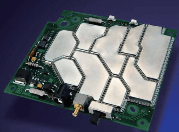
Rf pcb trace
Designing Efficient RF PCB Traces for High-Frequency Applications
Designing efficient RF PCB traces for high-frequency applications is a critical aspect of modern electronics engineering. As the demand for faster and more reliable wireless communication systems continues to grow, the need for precise and effective RF PCB trace design becomes increasingly important. This process involves a deep understanding of electromagnetic theory, material properties, and advanced fabrication techniques to ensure optimal performance.
To begin with, the selection of materials plays a pivotal role in the design of RF PCB traces.
High-frequency signals are particularly sensitive to the dielectric properties of the substrate material. Therefore, materials with low dielectric constant (Dk) and low loss tangent (Df) are preferred to minimize signal attenuation and phase distortion. Commonly used materials include PTFE (Polytetrafluoroethylene) and Rogers laminates, which offer excellent electrical performance at high frequencies.
Once the appropriate materials are selected, the next step involves the careful layout of the RF traces.
The width and spacing of the traces must be meticulously calculated to maintain the characteristic impedance, typically 50 ohms, which is crucial for minimizing signal reflections and ensuring signal integrity. Microstrip and stripline configurations are commonly used in RF PCB designs. Microstrip lines are placed on the outer layers of the PCB with a ground plane beneath them, while stripline traces are sandwiched between two ground planes, providing better shielding and reduced electromagnetic interference (EMI).
In addition to trace width and spacing, the routing of RF traces requires careful consideration.
Sharp bends and abrupt changes in trace width can cause impedance discontinuities, leading to signal reflections and loss. To mitigate these issues, designers often use gradual bends and maintain consistent trace widths throughout the signal path. Furthermore, the use of via transitions should be minimized, as they can introduce parasitic inductance and capacitance, adversely affecting the signal quality.
Another critical aspect of RF PCB trace design is the management of crosstalk and EMI.
High-frequency signals can easily couple with adjacent traces, leading to unwanted interference and signal degradation. To address this, designers implement proper spacing between RF traces and employ ground planes to provide effective shielding. Additionally, the use of guard traces, which are grounded traces placed between signal lines, can further reduce crosstalk and improve signal integrity.
Thermal management is also a key consideration in RF PCB design.
High-frequency components can generate significant heat, which can affect the performance and reliability of the PCB. To dissipate heat effectively, designers use thermal vias, heat sinks, and proper PCB stack-up configurations. Ensuring adequate thermal management not only enhances the performance of the RF traces but also prolongs the lifespan of the entire PCB.
Moreover, simulation and testing are indispensable steps in the design process.
Advanced simulation tools, such as electromagnetic field solvers, allow designers to model and analyze the behavior of RF traces under various conditions. These simulations help identify potential issues and optimize the design before fabrication. Once the PCB is manufactured, rigorous testing, including time-domain reflectometry (TDR) and vector network analysis (VNA), is conducted to verify the performance of the RF traces and ensure they meet the desired specifications.
In conclusion, designing efficient RF PCB traces for high-frequency applications requires a comprehensive understanding of material properties, precise layout techniques, and effective thermal management. By carefully considering these factors and utilizing advanced simulation and testing tools, engineers can create high-performance RF PCBs that meet the stringent demands of modern wireless communication systems.
Common Mistakes to Avoid in RF PCB Trace Layout
Designing RF PCB traces is a critical task that demands meticulous attention to detail. One common mistake in RF PCB trace layout is neglecting the importance of impedance matching. Impedance mismatches can lead to signal reflections, which degrade the performance of the RF circuit. To avoid this, designers must carefully calculate and maintain the characteristic impedance of the traces, ensuring it matches the source and load impedances. This often involves selecting the appropriate trace width and spacing, as well as considering the dielectric properties of the PCB material.
Another frequent error is improper grounding.
A solid and continuous ground plane is essential for minimizing noise and interference in RF circuits. Inadequate grounding can result in ground loops and increased electromagnetic interference (EMI), which can severely impact the signal integrity. Designers should ensure that the ground plane is as unbroken as possible and that all ground connections are short and direct. Additionally, using multiple vias to connect the ground plane to different layers can help maintain a low impedance path.
Transitioning to the topic of trace routing, it is crucial to avoid sharp bends in RF traces.
Sharp bends can cause impedance discontinuities and signal reflections, which degrade the performance of the RF circuit. Instead, designers should use gradual curves or mitered bends to maintain a consistent impedance along the trace. Furthermore, keeping the traces as short and direct as possible minimizes signal loss and reduces the potential for interference.
Another aspect to consider is the proximity of RF traces to other signal traces.
Placing RF traces too close to high-speed digital or power traces can result in crosstalk and EMI. To mitigate this, designers should maintain adequate spacing between RF traces and other signal paths. Additionally, using shielding techniques, such as ground traces or vias placed between RF and other signal traces, can help reduce interference.
Component placement is another area where mistakes are often made.
Placing components too far from the RF traces can introduce parasitic inductance and capacitance, which can affect the performance of the circuit. Designers should place components as close to the RF traces as possible, minimizing the length of the connecting traces. This is particularly important for components such as capacitors and inductors, which are used for impedance matching and filtering.
Thermal management is another critical consideration in RF PCB design.
High-frequency signals can generate significant heat, which can affect the performance and reliability of the circuit. Designers should ensure that there is adequate thermal relief for heat-generating components, such as power amplifiers. This may involve using thermal vias, heat sinks, or other cooling techniques to dissipate heat effectively.
Finally, it is essential to perform thorough testing and validation of the RF PCB design.
Simulation tools can help identify potential issues before the PCB is fabricated, but real-world testing is crucial for verifying the performance of the final design. Designers should use network analyzers, spectrum analyzers, and other RF testing equipment to measure parameters such as return loss, insertion loss, and signal integrity. By identifying and addressing any issues early in the design process, designers can ensure that the final product meets the required performance specifications.
In conclusion, avoiding common mistakes in RF PCB trace layout requires careful attention to impedance matching, grounding, trace routing, component placement, thermal management, and thorough testing. By adhering to these best practices, designers can create high-performance RF circuits that meet the stringent demands of modern applications.

Material Selection for Optimal RF PCB Trace Performance
When designing radio frequency (RF) printed circuit boards (PCBs), the selection of materials plays a pivotal role in ensuring optimal trace performance. The intricate nature of RF signals, which operate at high frequencies, necessitates a meticulous approach to material selection to mitigate signal loss, interference, and other performance-degrading factors. Consequently, understanding the properties of various materials and their impact on RF trace performance is essential for engineers and designers.
To begin with, the dielectric constant (Dk) of the substrate material is a critical parameter.
The dielectric constant affects the signal propagation speed and impedance of the RF traces. Materials with a low and stable dielectric constant are preferred because they minimize signal delay and ensure consistent impedance, which is crucial for maintaining signal integrity. Common materials such as FR-4, while cost-effective, have a relatively high and variable dielectric constant, making them less suitable for high-frequency applications. Instead, materials like Rogers RO4000 series, which offer a lower and more stable dielectric constant, are often chosen for RF PCB designs.
In addition to the dielectric constant, the loss tangent (Df) of the substrate material is another vital consideration.
The loss tangent measures the inherent energy loss of the material as the RF signal propagates through it. A lower loss tangent indicates less signal attenuation, which is particularly important for high-frequency applications where even minor losses can significantly impact performance. High-frequency laminates such as PTFE (Polytetrafluoroethylene) composites, known for their low loss tangent, are frequently employed in RF PCB designs to ensure minimal signal degradation.
Thermal management is another aspect that cannot be overlooked when selecting materials for RF PCB traces.
High-frequency signals can generate substantial heat, which, if not properly managed, can lead to performance issues and potential damage to the PCB. Materials with good thermal conductivity, such as ceramic-filled PTFE composites, help dissipate heat more effectively, thereby maintaining the reliability and longevity of the RF PCB.
Moreover, the coefficient of thermal expansion (CTE) of the substrate material must be compatible with the other components of the PCB.
A mismatch in CTE can lead to mechanical stresses during thermal cycling, potentially causing delamination or other structural failures. Materials with a low and matched CTE, such as certain ceramic-filled laminates, provide better dimensional stability and reliability under varying thermal conditions.
Surface roughness of the copper traces is another factor that influences RF performance.
Smoother copper surfaces reduce skin effect losses, which become more pronounced at higher frequencies. Advanced manufacturing techniques, such as using low-profile copper foils, can help achieve the desired surface smoothness, thereby enhancing signal integrity.
Furthermore, environmental considerations such as moisture absorption must be taken into account.
Materials that absorb moisture can experience changes in their dielectric properties, leading to unpredictable performance. Hydrophobic materials like PTFE are advantageous in such scenarios due to their low moisture absorption rates, ensuring consistent performance even in humid environments.
In conclusion, the selection of materials for RF PCB traces is a multifaceted process that requires careful consideration of various properties, including dielectric constant, loss tangent, thermal management, coefficient of thermal expansion, surface roughness, and environmental stability. By choosing materials that align with the specific requirements of high-frequency applications, engineers can optimize the performance, reliability, and longevity of RF PCBs, ultimately leading to more efficient and effective electronic systems.
Techniques for Minimizing Signal Loss in RF PCB Traces
In the realm of radio frequency (RF) design, minimizing signal loss in printed circuit board (PCB) traces is paramount to ensuring optimal performance. Signal loss, often referred to as attenuation, can significantly degrade the quality and efficiency of RF circuits. Therefore, employing effective techniques to mitigate this issue is crucial for engineers and designers.
One fundamental approach to minimizing signal loss in RF PCB traces is to carefully select the materials used in the PCB substrate. High-frequency signals are particularly sensitive to the dielectric properties of the substrate material. Low-loss materials, such as Rogers or Teflon-based laminates, exhibit lower dielectric constants and dissipation factors compared to standard FR-4 materials. These properties help reduce dielectric losses, thereby preserving signal integrity over longer distances.
Another critical technique involves optimizing the trace geometry. The width and thickness of the RF traces play a significant role in determining the characteristic impedance and, consequently, the signal loss. Wider traces tend to have lower resistance, which reduces ohmic losses. Additionally, maintaining a consistent trace width and avoiding abrupt changes in geometry can prevent impedance mismatches that lead to signal reflections and loss. Employing microstrip or stripline configurations, where the trace is either on the surface or sandwiched between layers of the PCB, can further enhance signal integrity by providing controlled impedance environments.
The use of proper grounding techniques is also essential in minimizing signal loss. A well-designed ground plane can significantly reduce electromagnetic interference (EMI) and crosstalk between adjacent traces. Ensuring a continuous and low-impedance ground path helps maintain signal integrity by providing a stable reference point for the RF signals. Additionally, incorporating via stitching, where multiple vias connect the ground plane to different layers, can further enhance the grounding effectiveness and reduce potential signal loss.
Moreover, the layout of the PCB traces should be meticulously planned to minimize signal loss. Keeping RF traces as short as possible reduces the potential for signal degradation. When longer traces are unavoidable, using techniques such as meandering or serpentine routing can help manage the trace length while maintaining a compact layout. Additionally, avoiding sharp bends and corners in the trace routing can prevent impedance discontinuities that contribute to signal loss.
The choice of connectors and components also plays a vital role in minimizing signal loss. High-quality RF connectors with low insertion loss and minimal reflection are essential for maintaining signal integrity. Similarly, selecting components with low parasitic elements, such as capacitors and inductors with minimal equivalent series resistance (ESR) and equivalent series inductance (ESL), can help reduce signal attenuation.
Furthermore, employing proper shielding techniques can significantly mitigate signal loss due to external interference. Shielding the RF traces with grounded metal enclosures or using coaxial cables for critical signal paths can effectively block unwanted electromagnetic radiation and prevent signal degradation. This is particularly important in environments with high levels of EMI, where unshielded traces are more susceptible to signal loss.
In conclusion, minimizing signal loss in RF PCB traces requires a comprehensive approach that encompasses material selection, trace geometry optimization, grounding techniques, meticulous layout planning, careful component selection, and effective shielding. By implementing these techniques, engineers can ensure that RF circuits operate with maximum efficiency and reliability, thereby achieving the desired performance in a wide range of applications.