Rf pcb prototyping
Essential Design Tips For RF PCB Prototyping
RF PCB prototyping is a critical phase in the development of radio frequency (RF) circuits, where precision and attention to detail are paramount. To ensure the success of your RF PCB prototype, it is essential to adhere to several design tips that can significantly impact performance and reliability.
One of the foremost considerations is the choice of substrate material.
The dielectric constant and loss tangent of the substrate can influence signal integrity and propagation speed. Materials such as Rogers or Teflon are often preferred for high-frequency applications due to their low dielectric losses and stable performance over a wide range of frequencies.
Transitioning from material selection, another crucial aspect is the layout of the PCB.
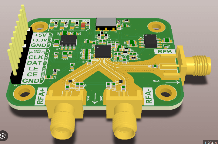
The layout must minimize signal loss and interference, which can be achieved by carefully planning the placement of components and routing of traces. It is advisable to keep signal paths as short as possible to reduce inductive and capacitive effects. Additionally, maintaining consistent trace widths and spacing is vital to ensure impedance matching, which is critical for minimizing reflections and signal degradation.
Furthermore, grounding plays a pivotal role in RF PCB design.
A well-designed ground plane can provide a low-impedance path for return currents, thereby reducing noise and improving signal integrity. It is recommended to use a solid ground plane and avoid splitting it, as discontinuities can lead to unwanted resonances and electromagnetic interference (EMI). Connecting the ground plane to the chassis ground at multiple points can also help in mitigating EMI.
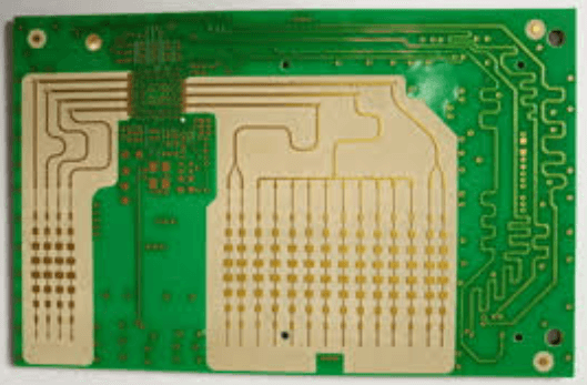
In addition to grounding, the use of vias must be judiciously managed.
Vias introduce inductance and can affect the performance of high-frequency signals. To minimize these effects, it is beneficial to use multiple vias for ground connections and to place them strategically to ensure a low-inductance path. Blind and buried vias can also be employed to reduce the impact on signal integrity.
Another essential design tip is the careful selection and placement of decoupling capacitors.
These capacitors are crucial for filtering out noise and providing a stable power supply to the RF components. Placing decoupling capacitors as close as possible to the power pins of active devices can significantly enhance performance. Additionally, using capacitors with low equivalent series resistance (ESR) and inductance (ESL) is recommended for high-frequency applications.
Thermal management is another critical consideration in RF PCB prototyping.
High-frequency components can generate significant heat, which can affect performance and reliability. Implementing thermal vias, heat sinks, and proper airflow can help in dissipating heat effectively. Ensuring that the PCB material has good thermal conductivity can also aid in managing heat dissipation.
Moreover, simulation and testing are indispensable steps in the RF PCB prototyping process.
Utilizing simulation tools can help in predicting the behavior of the circuit and identifying potential issues before fabrication. Post-fabrication testing, including impedance measurements and signal integrity analysis, is essential to verify that the prototype meets the desired specifications.
In conclusion, RF PCB prototyping demands meticulous attention to various design aspects, including substrate material selection, layout optimization, grounding, via management, decoupling capacitor placement, thermal management, and thorough testing. By adhering to these essential design tips, engineers can enhance the performance, reliability, and success of their RF PCB prototypes, paving the way for efficient and effective RF circuit development.
Common Challenges In RF PCB Prototyping And How To Overcome Them
RF PCB prototyping is a critical phase in the development of radio frequency circuits, which are integral to a wide range of applications, from telecommunications to medical devices. However, this process is fraught with challenges that can impede progress and affect the performance of the final product. Understanding these common challenges and knowing how to overcome them is essential for engineers and designers working in this field.
One of the primary challenges in RF PCB prototyping is signal integrity.
High-frequency signals are particularly susceptible to interference and loss, which can degrade performance. To mitigate this, careful attention must be paid to the layout of the PCB. Ensuring that signal paths are as short as possible and avoiding sharp bends can help maintain signal integrity. Additionally, using high-quality materials with low dielectric loss can further reduce signal degradation.
Another significant challenge is impedance matching.
Mismatched impedance can lead to reflections and standing waves, which can severely impact the performance of RF circuits. To address this, designers must carefully calculate and design the trace widths and spacing to match the impedance of the components and transmission lines. Utilizing simulation tools can aid in predicting and adjusting impedance characteristics before physical prototyping begins.
Thermal management is also a critical concern in RF PCB prototyping.
High-frequency components often generate significant heat, which can affect both the performance and longevity of the circuit. Effective thermal management strategies, such as incorporating thermal vias, heat sinks, and proper ventilation, are essential. Additionally, selecting components with appropriate thermal ratings and using materials with good thermal conductivity can help dissipate heat more efficiently.
Electromagnetic interference (EMI) poses another challenge in RF PCB prototyping.
EMI can originate from both external sources and within the circuit itself, leading to unwanted noise and signal disruption. Shielding techniques, such as using ground planes and metal enclosures, can help mitigate EMI. Furthermore, proper grounding and decoupling strategies are crucial to minimize the impact of EMI on the circuit’s performance.
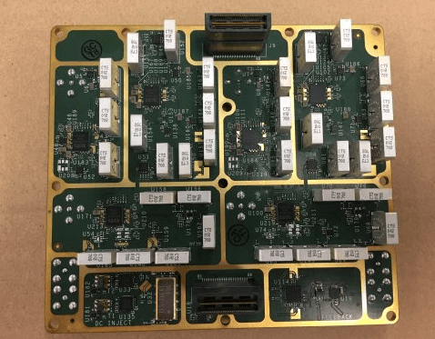
Component selection and placement are also critical factors in RF PCB prototyping.
The performance of RF circuits is highly dependent on the quality and characteristics of the components used. Selecting components with appropriate frequency ratings and low parasitic elements is essential. Additionally, the placement of components must be carefully considered to minimize parasitic inductance and capacitance, which can affect the circuit’s performance. Grouping related components together and maintaining adequate spacing can help achieve optimal performance.
Moreover, the manufacturing process itself can introduce challenges in RF PCB prototyping.
Variations in the fabrication process, such as etching tolerances and layer alignment, can affect the final performance of the PCB. Working closely with experienced manufacturers and specifying tight tolerances can help ensure that the prototype meets the desired specifications. Additionally, conducting thorough testing and validation of the prototype is essential to identify and address any issues before moving to mass production.
In conclusion, RF PCB prototyping presents a unique set of challenges that require careful consideration and meticulous planning. By addressing issues related to signal integrity, impedance matching, thermal management, EMI, component selection, and manufacturing processes, designers can overcome these challenges and develop high-performance RF circuits. Leveraging advanced simulation tools, collaborating with experienced manufacturers, and conducting thorough testing are key strategies to ensure the success of RF PCB prototyping projects.
Materials And Tools Required For Effective RF PCB Prototyping
RF PCB prototyping is a critical process in the development of high-frequency electronic circuits, and it requires a meticulous selection of materials and tools to ensure optimal performance. The materials and tools chosen can significantly impact the functionality, reliability, and efficiency of the final product. Therefore, understanding the essential components and equipment is paramount for anyone involved in RF PCB prototyping.
To begin with, the substrate material is a fundamental consideration in RF PCB prototyping.
The substrate serves as the foundation of the PCB and must posselso vital.
The copper layer on the PCB must be of high purity and uniform thickness to ensure consistent signal transmission. Typically, copper with a thickness of 1 oz/ft² is used, but for specific high-frequency applications, thinner or thicker copper layers may be required. The quality of the copper cladding directly affects the impedance control and overall performance of the RF PCB.
Moving on to the tools required, precision is key in RF PCB prototyping.
One of the most important tools is a high-resolution PCB printer or plotter. This equipment is used to create the intricate patterns required for RF circuits. The printer must be capable of producing fine lines and spaces with high accuracy to ensure the proper functioning of the circuit. Additionally, a laser cutter or CNC milling machine is often employed to cut and shape the PCB with precision. These machines allow for the creation of complex geometries and ensure that the physical dimensions of the PCB match the design specifications.
Furthermore, soldering equipment is essential for assembling the components onto the PCB. A high-quality soldering iron with temperature control is necessary to avoid damaging sensitive RF components. Solder paste and flux are also required to ensure strong and reliable connections. For more advanced prototyping, reflow ovens and pick-and-place machines can be used to automate the assembly process, providing greater consistency and efficiency.
Testing and measurement tools are equally important in RF PCB prototyping.
A vector network analyzer (VNA) is a critical instrument for measuring the performance of RF circuits. It allows for the characterization of parameters such as return loss, insertion loss, and impedance matching. Additionally, spectrum analyzers and oscilloscopes are used to analyze signal integrity and detect any anomalies in the circuit. These tools provide valuable insights into the behavior of the RF PCB and help identify any issues that need to be addressed.
In conclusion, effective RF PCB prototyping requires a careful selection of materials and tools. The choice of substrate and copper cladding plays a crucial role in ensuring signal integrity, while precision equipment such as high-resolution printers, laser cutters, and soldering tools are essential for accurate fabrication and assembly. Testing and measurement instruments like VNAs, spectrum analyzers, and oscilloscopes are indispensable for validating the performance of the RF PCB. By paying close attention to these factors, one can achieve a successful RF PCB prototype that meets the stringent demands of high-frequency applications.
Innovative Techniques For High-Frequency RF PCB Prototyping
In the realm of high-frequency RF PCB prototyping, innovative techniques are continually being developed to meet the increasing demands for performance, reliability, and miniaturization. As the complexity of RF circuits grows, so does the need for advanced methods that can ensure precision and efficiency in the prototyping process.
One of the primary challenges in RF PCB prototyping is managing signal integrity,
which is crucial for maintaining the performance of high-frequency circuits. To address this, designers are increasingly turning to advanced simulation tools that allow for meticulous planning and analysis before physical prototyping begins. These tools enable the identification and mitigation of potential issues such as signal loss, crosstalk, and electromagnetic interference (EMI), which are particularly problematic at high frequencies.
Moreover, the choice of materials plays a pivotal role in the success of RF PCB prototypes.
Traditional FR-4 substrates, while cost-effective, often fall short in high-frequency applications due to their higher dielectric losses. Consequently, materials such as Rogers, Taconic, and other low-loss laminates are preferred for their superior electrical properties. These materials help to minimize signal attenuation and ensure that the PCB can handle the stringent requirements of RF applications. Additionally, the use of advanced materials necessitates precise manufacturing techniques to maintain the integrity of the design.
Another innovative technique gaining traction is the use of multilayer PCBs.
By incorporating multiple layers, designers can achieve greater component density and improved signal routing, which is essential for high-frequency applications. Multilayer PCBs also allow for better isolation of RF signals from other circuit elements, thereby reducing the risk of interference. However, the complexity of multilayer designs requires careful consideration of factors such as layer stack-up, via placement, and impedance control to ensure optimal performance.
Furthermore, the advent of additive manufacturing, or 3D printing, has opened new avenues for RF PCB prototyping.
This technology allows for rapid prototyping and iterative testing, which can significantly shorten development cycles. 3D printing also offers the flexibility to create complex geometries that would be challenging or impossible to achieve with traditional manufacturing methods. As a result, designers can experiment with novel structures and materials to optimize the performance of their RF circuits.
In addition to these techniques, the integration of surface-mount technology (SMT) has revolutionized the assembly process for RF PCBs.
SMT allows for the placement of smaller, more efficient components directly onto the surface of the PCB, reducing parasitic inductance and capacitance that can degrade high-frequency signals. This method also supports automated assembly processes, which enhance precision and repeatability, further contributing to the reliability of the final product.
Lastly, rigorous testing and validation are indispensable components of the RF PCB prototyping process.
Techniques such as vector network analysis, time-domain reflectometry, and spectrum analysis are employed to verify the performance of the prototype under real-world conditions. These tests help to identify any discrepancies between the simulated and actual performance, allowing for necessary adjustments to be made before mass production.
In conclusion, the field of high-frequency RF PCB prototyping is characterized by a continuous evolution of techniques aimed at overcoming the inherent challenges of high-frequency design. Through the use of advanced simulation tools, superior materials, multilayer designs, additive manufacturing, surface-mount technology, and comprehensive testing, designers are better equipped than ever to create reliable and high-performing RF circuits. As technology progresses, these innovative techniques will undoubtedly continue to advance, paving the way for even more sophisticated and efficient RF PCB prototypes.