Rf pcb impedance matching
Understanding The Basics Of RF PCB Impedance Matching
Impedance matching is a critical aspect of designing Radio Frequency (RF) Printed Circuit Boards (PCBs). It ensures that the maximum amount of power is transferred from the source to the load, minimizing reflections and signal loss. Understanding the basics of RF PCB impedance matching is essential for engineers and designers who aim to optimize the performance of their RF circuits.
At its core, impedance matching involves making the impedance of the source equal to the impedance of the load.
This is particularly important in RF circuits, where high-frequency signals are more susceptible to reflections and losses. When the impedances are mismatched, part of the signal is reflected back to the source, causing interference and reducing the efficiency of the system. Therefore, achieving proper impedance matching is crucial for maintaining signal integrity and ensuring efficient power transfer.
One of the fundamental concepts in impedance matching is the characteristic impedance of transmission lines.
In RF PCB design, transmission lines are used to route high-frequency signals between different components. The characteristic impedance of a transmission line is determined by its physical dimensions and the dielectric properties of the materials used. Common types of transmission lines include microstrip lines, stripline, and coplanar waveguides, each with its own characteristic impedance.
To achieve impedance matching, designers often use matching networks, which are circuits designed to transform the impedance of the source to match the impedance of the load.
These networks can be implemented using various components such as resistors, capacitors, and inductors. The choice of components and the configuration of the matching network depend on the specific requirements of the RF circuit and the frequency range of operation.
One common method for impedance matching is the use of a quarter-wave transformer.
This technique involves using a transmission line with a length equal to one-quarter of the wavelength of the signal. The characteristic impedance of this transmission line is chosen to be the geometric mean of the source and load impedances. When the signal travels through the quarter-wave transformer, it undergoes a transformation that matches the impedances, minimizing reflections and maximizing power transfer.
Another widely used technique is the use of lumped element matching networks.
These networks consist of discrete components such as capacitors and inductors arranged in specific configurations. The most common configurations are the L-network, T-network, and Pi-network. Each configuration has its own advantages and is chosen based on the specific requirements of the RF circuit. For example, the L-network is simple and easy to design, while the Pi-network provides better performance over a wider frequency range.
In addition to these techniques, modern RF PCB design tools offer simulation capabilities that allow designers to model and analyze the impedance matching of their circuits.
These tools can simulate the behavior of transmission lines and matching networks, providing valuable insights into the performance of the RF circuit. By using these tools, designers can optimize their designs and ensure proper impedance matching before manufacturing the PCB.
In conclusion, understanding the basics of RF PCB impedance matching is essential for designing efficient and high-performance RF circuits. By ensuring that the impedances of the source and load are matched, designers can minimize reflections, reduce signal loss, and maximize power transfer. Techniques such as quarter-wave transformers and lumped element matching networks, along with modern simulation tools, provide designers with the necessary tools to achieve proper impedance matching in their RF PCB designs.
Techniques For Accurate Impedance Matching In RF PCB Design
Impedance matching is a critical aspect of RF PCB design, ensuring that the maximum amount of power is transferred from the source to the load with minimal reflection and loss. Achieving accurate impedance matching requires a comprehensive understanding of various techniques and principles. One fundamental technique involves the use of transmission lines, which are designed to have a characteristic impedance that matches the source and load impedances. This can be accomplished by carefully selecting the width and spacing of the traces on the PCB, as well as the dielectric constant of the substrate material.
Another essential technique is the use of impedance matching networks, which can be implemented using discrete components such as resistors, capacitors, and inductors.
These networks are designed to transform the impedance of the source or load to match the desired value. For instance, a simple L-network, consisting of a series inductor and a parallel capacitor, can be used to match a high impedance source to a low impedance load. More complex matching networks, such as pi-networks and T-networks, can provide greater flexibility and bandwidth.
In addition to transmission lines and matching networks, the use of Smith charts is invaluable for visualizing and solving impedance matching problems.
The Smith chart is a graphical tool that represents complex impedance and reflection coefficients, allowing designers to plot the impedance of various components and trace the effects of adding matching elements. By using the Smith chart, designers can quickly identify the appropriate values for inductors and capacitors to achieve the desired impedance match.
Furthermore, the choice of materials and manufacturing processes plays a significant role in achieving accurate impedance matching.
High-frequency PCBs often require substrates with low dielectric loss and stable dielectric constants, such as PTFE or ceramic-filled laminates. These materials help maintain consistent impedance characteristics across the operating frequency range. Additionally, precise control of trace dimensions and spacing during the manufacturing process is crucial to ensure that the designed impedance values are accurately realized in the final PCB.
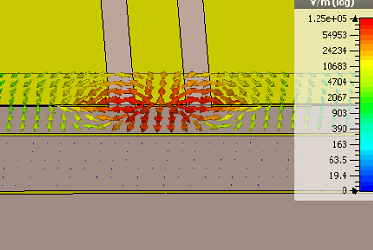
Simulation tools are also indispensable in the design process, enabling designers to model and analyze the impedance characteristics of their PCB layouts before fabrication.
Electromagnetic simulation software can predict the behavior of transmission lines and matching networks, allowing for optimization and validation of the design. By iterating through simulations, designers can fine-tune their layouts to achieve the desired impedance matching with high accuracy.
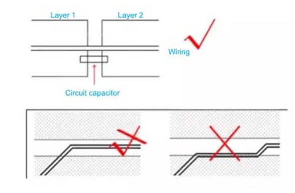
Moreover, it is essential to consider the impact of parasitic elements, such as stray capacitance and inductance, which can affect the impedance matching performance.
These parasitics can arise from various sources, including component leads, vias, and PCB layout features. Careful layout practices, such as minimizing lead lengths and using ground planes, can help mitigate the effects of parasitics and improve the overall impedance matching.
Finally, testing and measurement are crucial steps in verifying the impedance matching of an RF PCB design.
Vector network analyzers (VNAs) are commonly used to measure the impedance and reflection coefficients of the PCB, providing valuable feedback for further refinement. By comparing the measured results with the simulated predictions, designers can identify any discrepancies and make necessary adjustments to achieve optimal impedance matching.
In conclusion, accurate impedance matching in RF PCB design requires a combination of techniques, including the use of transmission lines, matching networks, Smith charts, careful material selection, precise manufacturing, simulation tools, and thorough testing. By employing these techniques, designers can ensure efficient power transfer and minimal signal reflection, leading to improved performance and reliability of RF circuits.
Common Challenges And Solutions In RF PCB Impedance Matching
Impedance matching in RF PCB design is a critical aspect that ensures the efficient transmission of signals with minimal reflection and loss. One of the most common challenges in RF PCB impedance matching is the variation in impedance due to manufacturing tolerances. Even slight deviations in the width of a trace or the dielectric constant of the substrate can lead to significant impedance mismatches. To mitigate this, designers often employ controlled impedance techniques, which involve specifying the exact dimensions and materials to be used. This requires close collaboration with the PCB manufacturer to ensure that the design specifications are met accurately.
Another prevalent issue is the parasitic effects that arise from the physical layout of the PCB.
Parasitic inductance and capacitance can distort the signal, leading to impedance mismatches. To address this, designers must carefully consider the placement and routing of traces. For instance, keeping signal traces as short as possible and avoiding sharp bends can help minimize parasitic effects. Additionally, the use of ground planes and proper via placement can further reduce these unwanted parasitics, thereby improving impedance matching.
The choice of components also plays a crucial role in impedance matching.
Components such as resistors, capacitors, and inductors have their own inherent impedance characteristics, which can affect the overall impedance of the circuit. Selecting components with tight tolerance specifications and placing them strategically within the circuit can help achieve better impedance matching. Moreover, using simulation tools to model the impedance characteristics of the entire circuit, including the components, can provide valuable insights and allow for adjustments before the actual fabrication.
Thermal effects are another factor that can impact impedance matching.
Changes in temperature can alter the electrical properties of the materials used in the PCB, leading to impedance variations. To counteract this, designers can use materials with low thermal coefficients and ensure that the PCB operates within a stable temperature range. Additionally, thermal management techniques such as heat sinks and thermal vias can help maintain consistent operating conditions, thereby minimizing impedance fluctuations.
Signal integrity is closely linked to impedance matching, and issues such as crosstalk and electromagnetic interference (EMI) can further complicate the design process.
Crosstalk occurs when signals in adjacent traces interfere with each other, while EMI involves external sources disrupting the signal. To mitigate these issues, designers can use differential signaling, which involves using pairs of traces to carry the signal and its inverse. This technique helps cancel out noise and improves impedance matching. Shielding and proper grounding techniques can also be employed to reduce EMI and enhance signal integrity.
Finally, testing and validation are essential steps in ensuring effective impedance matching.
Using tools such as vector network analyzers (VNAs) and time-domain reflectometers (TDRs), designers can measure the impedance characteristics of the PCB and identify any mismatches. These measurements can then be used to fine-tune the design, making necessary adjustments to achieve optimal impedance matching.
In conclusion, RF PCB impedance matching presents several challenges, including manufacturing tolerances, parasitic effects, component selection, thermal effects, and signal integrity issues. By employing controlled impedance techniques, careful layout design, strategic component placement, thermal management, and thorough testing, designers can overcome these challenges and achieve efficient impedance matching. This ensures the reliable transmission of RF signals, which is crucial for the performance of modern electronic devices.
The Role Of Simulation Tools In RF PCB Impedance Matching
In the realm of radio frequency (RF) printed circuit board (PCB) design, impedance matching is a critical aspect that ensures signal integrity and optimal performance. The process of impedance matching involves adjusting the impedance of the transmission line to match the source and load impedances, thereby minimizing signal reflection and power loss. As RF designs become increasingly complex, the role of simulation tools in achieving precise impedance matching has become indispensable.
Simulation tools offer a virtual environment where designers can model and analyze the behavior of RF circuits before physical prototypes are built.
This capability is particularly valuable in impedance matching, as it allows for the identification and mitigation of potential issues early in the design process. By using simulation tools, designers can experiment with different configurations and components to achieve the desired impedance characteristics without the time and cost associated with iterative physical testing.
One of the primary advantages of simulation tools is their ability to provide detailed insights into the electromagnetic behavior of RF circuits.
These tools utilize advanced algorithms to simulate the propagation of RF signals through various materials and geometries, enabling designers to visualize how changes in the PCB layout affect impedance. For instance, simulation tools can model the effects of trace width, spacing, and dielectric constant on the impedance of transmission lines. This level of detail is crucial for fine-tuning the design to meet stringent impedance requirements.
Moreover, simulation tools facilitate the optimization of matching networks, which are essential components in RF circuits.
Matching networks, composed of inductors, capacitors, and resistors, are used to transform impedances to achieve maximum power transfer. Through simulation, designers can evaluate different network topologies and component values to determine the most effective configuration. This process not only enhances the accuracy of impedance matching but also reduces the risk of performance degradation due to component tolerances and variations.
In addition to optimizing individual components, simulation tools enable the comprehensive analysis of the entire RF system.
This holistic approach is vital for ensuring that impedance matching is maintained across all stages of the signal path, from the antenna to the receiver. By simulating the complete system, designers can identify and address impedance mismatches that may arise from interactions between different circuit elements. This capability is particularly important in modern RF designs, where multiple frequency bands and signal paths are often integrated into a single PCB.
Furthermore, simulation tools support the iterative nature of the design process by providing rapid feedback on design changes.
This iterative approach allows designers to refine their impedance matching strategies based on real-time simulation results. For example, if a simulation reveals an impedance mismatch at a specific frequency, designers can quickly adjust the layout or component values and re-simulate to verify the improvement. This iterative cycle significantly accelerates the design process and enhances the likelihood of achieving optimal impedance matching.
In conclusion, the role of simulation tools in RF PCB impedance matching cannot be overstated. These tools provide a powerful means of modeling, analyzing, and optimizing RF circuits, enabling designers to achieve precise impedance matching with greater efficiency and accuracy. By leveraging the capabilities of simulation tools, designers can ensure that their RF designs meet performance specifications and operate reliably in real-world applications. As RF technology continues to evolve, the importance of simulation tools in the design process will only continue to grow, underscoring their essential role in the advancement of RF PCB design.