Que significa pcb assembly
Understanding The Basics Of PCB Assembly
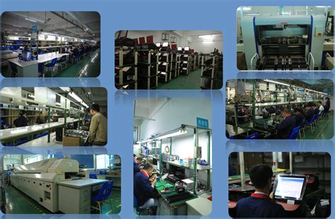
PCB assembly, or Printed Circuit Board assembly, is a critical process in the manufacturing of electronic devices. It involves the integration of electronic components onto a PCB to create a functional electronic circuit. Understanding the basics of PCB assembly is essential for anyone involved in electronics design, manufacturing, or repair.
To begin with, a PCB serves as the foundation for electronic circuits.
It is typically made of a non-conductive substrate, such as fiberglass, with conductive pathways etched or printed onto its surface. These pathways, often referred to as traces, connect various electronic components, allowing them to communicate and function together. The assembly process transforms a bare PCB into a fully operational electronic device by attaching components like resistors, capacitors, integrated circuits, and connectors.
The PCB assembly process can be divided into several key stages.
Initially, the design phase involves creating a schematic diagram and layout for the PCB. This design is then translated into a set of manufacturing files, which guide the production of the bare PCB. Once the PCB is fabricated, the assembly process begins with the application of solder paste to the board. Solder paste, a mixture of tiny solder balls and flux, is applied to the areas where components will be placed. This step is typically performed using a stencil and a squeegee to ensure precise application.
Following the application of solder paste, the next step is component placement.
This is often done using automated machines known as pick-and-place machines, which accurately position components onto the PCB based on the design files. These machines are capable of placing components with high precision and speed, making them indispensable in modern PCB assembly.
Once the components are in place, the assembly undergoes a reflow soldering process.
During reflow soldering, the PCB is passed through a reflow oven, where it is gradually heated to melt the solder paste. As the solder cools, it solidifies, creating strong electrical and mechanical connections between the components and the PCB. This process ensures that the components are securely attached and that the circuit functions as intended.
After reflow soldering, the assembled PCB is inspected for any defects or issues.
This inspection can be performed using various methods, including automated optical inspection (AOI), X-ray inspection, and manual visual inspection. These techniques help identify problems such as solder bridges, misaligned components, or incomplete solder joints, which can affect the performance and reliability of the final product.
In some cases, additional assembly steps may be required, such as through-hole component insertion and wave soldering.
Through-hole components have leads that pass through holes in the PCB and are soldered on the opposite side. Wave soldering involves passing the PCB over a wave of molten solder to attach these components. This method is particularly useful for components that cannot be easily placed using surface-mount technology (SMT).
Finally, the assembled PCB undergoes functional testing to ensure that it operates correctly.
This testing can include in-circuit testing (ICT), which checks individual components and connections, as well as functional testing, which verifies the overall performance of the assembled device. Any issues identified during testing are addressed through rework or repair processes.
In conclusion, PCB assembly is a complex and multifaceted process that transforms a bare PCB into a functional electronic device. It involves several stages, including design, solder paste application, component placement, reflow soldering, inspection, and testing. Understanding these basics is crucial for anyone involved in the electronics industry, as it ensures the production of reliable and high-quality electronic products.
Key Components In PCB Assembly
PCB assembly, or Printed Circuit Board assembly, is a critical process in the manufacturing of electronic devices. It involves the integration of various electronic components onto a PCB to create a functional electronic circuit. Understanding the key components involved in PCB assembly is essential for grasping the complexity and precision required in this field.
To begin with, the PCB itself serves as the foundation for the entire assembly process.
It is typically made of a non-conductive substrate, such as fiberglass, with conductive pathways etched or printed onto its surface. These pathways, often referred to as traces, allow for the electrical connection between different components. The design and layout of the PCB are crucial, as they determine the efficiency and functionality of the final product.
Moving on, one of the primary components in PCB assembly is the surface-mount device (SMD).
SMDs are electronic components that are mounted directly onto the surface of the PCB. They are preferred over traditional through-hole components due to their smaller size and higher component density, which allows for more compact and efficient designs. Common SMDs include resistors, capacitors, diodes, and integrated circuits (ICs). The placement of these components is typically done using automated machines, ensuring precision and consistency.
In addition to SMDs, through-hole components also play a significant role in PCB assembly.
These components have leads that pass through holes in the PCB and are soldered onto the opposite side. While they are bulkier than SMDs, through-hole components are often used for parts that require a stronger mechanical bond, such as connectors and large capacitors. The combination of SMD and through-hole components allows for a versatile and robust PCB design.
Another critical aspect of PCB assembly is the soldering process.
Soldering involves the use of a metal alloy, known as solder, to create a permanent electrical connection between components and the PCB. There are two primary soldering techniques: reflow soldering and wave soldering. Reflow soldering is commonly used for SMDs and involves applying solder paste to the PCB, placing the components, and then heating the assembly in a reflow oven to melt the solder and secure the components. Wave soldering, on the other hand, is used for through-hole components and involves passing the PCB over a wave of molten solder to create the necessary connections.
Furthermore, the inspection and testing of assembled PCBs are crucial to ensure their functionality and reliability.
Automated optical inspection (AOI) systems are often employed to check for defects such as misaligned components, solder bridges, and insufficient solder joints. Additionally, in-circuit testing (ICT) and functional testing are performed to verify the electrical performance of the assembled PCB. These tests help identify any issues early in the production process, reducing the risk of faulty products reaching the market.
Lastly, the final step in PCB assembly is the application of a protective coating, known as conformal coating.
This coating protects the PCB from environmental factors such as moisture, dust, and chemicals, which can degrade its performance over time. The conformal coating is typically applied using methods such as spraying, dipping, or brushing, ensuring that all components are adequately covered.
In conclusion, PCB assembly is a multifaceted process that involves the integration of various key components, including the PCB itself, SMDs, through-hole components, and soldering techniques. The precision and reliability of this process are ensured through rigorous inspection and testing, culminating in the application of a protective conformal coating. Understanding these components and their roles is essential for appreciating the complexity and importance of PCB assembly in the manufacturing of electronic devices.
The Importance Of Quality Control In PCB Assembly
In the realm of electronics manufacturing, the term “PCB assembly” refers to the process of soldering electronic components onto a printed circuit board (PCB) to create a functional electronic device. This intricate procedure is fundamental to the production of virtually all electronic gadgets, from simple household appliances to complex aerospace systems. Given the critical role that PCBs play in the functionality and reliability of these devices, the importance of quality control in PCB assembly cannot be overstated.
Quality control in PCB assembly encompasses a series of meticulous checks and balances designed to ensure that each board meets stringent performance and reliability standards.
This process begins with the inspection of raw materials, including the PCB substrate and electronic components, to verify their compliance with specified quality criteria. By ensuring that only high-quality materials are used, manufacturers can significantly reduce the risk of defects and failures in the final product.
As the assembly process progresses, various stages of inspection and testing are employed to identify and rectify potential issues.
For instance, automated optical inspection (AOI) systems are commonly used to examine solder joints and component placements for any discrepancies. These systems utilize high-resolution cameras and advanced algorithms to detect even the smallest deviations from the intended design, thereby ensuring that each board is assembled with precision.
In addition to AOI, in-circuit testing (ICT) is another critical quality control measure.
ICT involves the use of specialized test fixtures and probes to evaluate the electrical performance of the assembled PCB. By applying test signals to various points on the board, ICT can identify issues such as short circuits, open circuits, and incorrect component values. This level of scrutiny is essential for verifying that the PCB will function correctly in its intended application.
Moreover, functional testing is often employed as a final quality control step.
This involves subjecting the assembled PCB to real-world operating conditions to ensure that it performs as expected. Functional testing can include a range of assessments, from simple power-on tests to complex simulations of the device’s intended use. By thoroughly vetting each board in this manner, manufacturers can provide a high level of assurance that the final product will meet or exceed customer expectations.
The importance of quality control in PCB assembly extends beyond the immediate goal of producing reliable electronic devices.
It also has significant implications for a manufacturer’s reputation and bottom line. High-quality PCBs are less likely to fail in the field, which can reduce warranty claims and costly recalls. Furthermore, consistent quality can enhance customer satisfaction and foster long-term business relationships.
In conclusion, quality control is an indispensable aspect of PCB assembly that ensures the reliability and performance of electronic devices. Through rigorous inspection and testing at every stage of the assembly process, manufacturers can identify and address potential issues before they become critical problems. This not only safeguards the functionality of the final product but also contributes to the overall success and reputation of the manufacturer. As the demand for advanced electronic devices continues to grow, the emphasis on quality control in PCB assembly will remain a cornerstone of the electronics manufacturing industry.
Common Challenges In PCB Assembly And How To Overcome Them
PCB assembly, or Printed Circuit Board assembly, is a critical process in the manufacturing of electronic devices. It involves the placement and soldering of electronic components onto a PCB, which serves as the foundation for the electronic circuitry. Despite its importance, PCB assembly is fraught with numerous challenges that can impact the quality and functionality of the final product. Understanding these common challenges and how to overcome them is essential for ensuring a successful assembly process.
One of the primary challenges in PCB assembly is component placement accuracy.
With the increasing miniaturization of electronic components, precise placement has become more critical than ever. Misaligned components can lead to poor electrical connections, resulting in device malfunction or failure. To address this issue, manufacturers often employ advanced pick-and-place machines equipped with high-resolution cameras and sophisticated algorithms. These machines can accurately position components on the PCB, significantly reducing the risk of misalignment.
Another significant challenge is soldering defects, which can manifest as solder bridges, cold joints, or insufficient solder.
Solder bridges occur when excess solder creates an unintended connection between two adjacent pads, leading to short circuits. Cold joints, on the other hand, are weak connections caused by insufficient heat during the soldering process. Insufficient solder can result in poor electrical connectivity and mechanical strength. To mitigate these issues, manufacturers can implement stringent process controls, such as optimizing solder paste application, reflow oven profiles, and using automated optical inspection (AOI) systems to detect and correct defects early in the process.
Thermal management is also a critical concern in PCB assembly.
As electronic devices become more powerful and compact, they generate more heat, which can adversely affect performance and longevity. Effective thermal management involves designing PCBs with adequate heat dissipation mechanisms, such as thermal vias, heat sinks, and proper component placement. Additionally, using materials with high thermal conductivity and ensuring proper airflow within the device can help manage heat more effectively.
Component availability and supply chain issues present another challenge in PCB assembly.
The global electronics industry is highly dynamic, with frequent changes in component availability and lead times. Shortages or delays in obtaining critical components can disrupt production schedules and increase costs. To overcome this challenge, manufacturers can adopt strategies such as maintaining a diversified supplier base, keeping safety stock of critical components, and using alternative or equivalent parts when necessary. Additionally, fostering strong relationships with suppliers can provide better visibility into potential supply chain disruptions and allow for more proactive planning.
Quality control is paramount in PCB assembly, as even minor defects can lead to significant issues in the final product.
Implementing a robust quality management system (QMS) that includes regular inspections, testing, and process audits can help identify and address potential problems early. Techniques such as in-circuit testing (ICT), functional testing, and X-ray inspection can provide valuable insights into the integrity of the assembled PCBs.
In conclusion, while PCB assembly presents several challenges, understanding and addressing these issues through advanced technology, stringent process controls, effective thermal management, proactive supply chain strategies, and robust quality control can significantly enhance the reliability and performance of electronic devices. By continuously improving these aspects, manufacturers can ensure that their PCB assemblies meet the high standards required in today’s competitive electronics market.