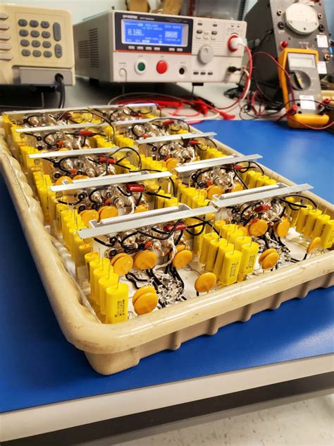
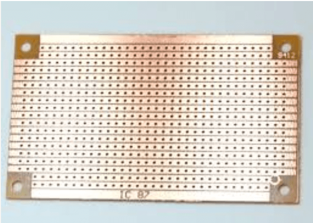
Printed circuit board use
Advantages Of Using Printed Circuit Boards In Modern Electronics
Printed circuit boards (PCBs) have become an indispensable component in modern electronics, offering a multitude of advantages that have revolutionized the way electronic devices are designed, manufactured, and utilized. One of the primary benefits of using PCBs is their ability to provide a compact and organized platform for electronic components. By embedding conductive pathways within a non-conductive substrate, PCBs eliminate the need for complex wiring, thereby reducing the overall size and weight of electronic devices. This miniaturization is particularly crucial in the development of portable gadgets such as smartphones, tablets, and wearable technology, where space is at a premium.
In addition to their compactness, PCBs offer enhanced reliability and durability.
The fixed layout of components on a PCB ensures consistent performance and reduces the likelihood of connection failures that can occur with traditional wiring methods. The use of high-quality materials and advanced manufacturing techniques further contributes to the longevity of PCBs, making them suitable for applications in harsh environments, such as automotive and aerospace industries. Moreover, the ability to incorporate multiple layers in a single PCB allows for more complex and sophisticated circuit designs, enabling the development of advanced electronic systems with greater functionality.
Another significant advantage of PCBs is their cost-effectiveness in mass production.
Once a PCB design is finalized, it can be easily replicated using automated manufacturing processes, resulting in significant economies of scale. This not only lowers the production costs but also ensures uniformity and consistency across all units. The standardization of PCBs also simplifies the assembly process, as components can be easily mounted and soldered onto the board using automated equipment. This reduces labor costs and minimizes the risk of human error, further enhancing the overall efficiency of the manufacturing process.
PCBs also play a crucial role in improving the performance and efficiency of electronic devices.
The precise arrangement of components and conductive pathways on a PCB minimizes electrical noise and interference, leading to better signal integrity and faster data transmission. This is particularly important in high-frequency applications, such as telecommunications and computing, where even minor disruptions can significantly impact performance. Additionally, the use of PCBs allows for better thermal management, as heat generated by components can be effectively dissipated through the board, preventing overheating and ensuring optimal operation.
Furthermore, the versatility of PCBs makes them suitable for a wide range of applications.
From consumer electronics and medical devices to industrial machinery and military equipment, PCBs are integral to the functioning of countless electronic systems. Their ability to support various types of components, including resistors, capacitors, and integrated circuits, allows for the creation of diverse and complex electronic solutions tailored to specific needs. This adaptability is further enhanced by the availability of different types of PCBs, such as single-sided, double-sided, and multi-layered boards, each offering unique advantages for different applications.
In conclusion, the advantages of using printed circuit boards in modern electronics are manifold. Their compactness, reliability, cost-effectiveness, performance enhancement, and versatility make them an essential component in the design and manufacture of contemporary electronic devices. As technology continues to advance, the role of PCBs is likely to become even more critical, driving innovation and enabling the development of increasingly sophisticated and efficient electronic systems.
The Role Of Printed Circuit Boards In IoT Devices
Printed circuit boards (PCBs) have become indispensable in the realm of modern electronics, particularly in the burgeoning field of the Internet of Things (IoT). As IoT devices proliferate, the role of PCBs in these applications has grown exponentially, serving as the backbone that supports the intricate web of connectivity and functionality. To understand the significance of PCBs in IoT devices, it is essential to explore their fundamental contributions to the design, performance, and reliability of these interconnected systems.
At the core of any IoT device lies the PCB, which provides the physical platform for mounting and interconnecting various electronic components.
These components include microcontrollers, sensors, communication modules, and power management units, all of which are crucial for the device’s operation. The PCB not only facilitates the electrical connections between these components but also ensures their mechanical stability. This dual role is particularly important in IoT devices, which often operate in diverse and sometimes harsh environments, necessitating robust and reliable construction.
Moreover, the miniaturization of electronic components has allowed for the development of compact and efficient PCBs, which are essential for IoT devices that prioritize space-saving and portability.
The ability to integrate multiple functions onto a single PCB has enabled the creation of sophisticated IoT devices that can perform complex tasks while maintaining a small form factor. This miniaturization is achieved through advanced PCB design techniques, such as multi-layered boards and surface-mount technology, which allow for higher component density and improved performance.
In addition to their structural and electrical roles, PCBs play a critical part in the thermal management of IoT devices.
As electronic components generate heat during operation, effective heat dissipation is necessary to maintain optimal performance and prevent damage. PCBs are designed with thermal management features, such as heat sinks, thermal vias, and conductive materials, to efficiently dissipate heat away from sensitive components. This ensures the longevity and reliability of IoT devices, which are often expected to operate continuously over extended periods.
Furthermore, the versatility of PCBs allows for the integration of various communication technologies, which are fundamental to the functionality of IoT devices.
Whether it is Wi-Fi, Bluetooth, Zigbee, or cellular connectivity, PCBs can accommodate the necessary communication modules and antennas, enabling seamless data transmission and reception. This connectivity is the cornerstone of IoT, as it allows devices to interact with each other and with centralized systems, facilitating the collection, analysis, and utilization of data.
The role of PCBs in IoT devices extends beyond their physical and functional attributes to encompass considerations of manufacturability and cost-effectiveness.
The design and production of PCBs must balance performance requirements with economic constraints, ensuring that IoT devices are both high-performing and affordable. Advances in PCB manufacturing technologies, such as automated assembly and testing, have streamlined production processes, reducing costs and improving quality. This has made it feasible to produce IoT devices at scale, accelerating their adoption across various industries.
In conclusion, printed circuit boards are integral to the development and operation of IoT devices, providing the essential infrastructure for mounting components, managing heat, enabling connectivity, and ensuring reliability. As the IoT landscape continues to evolve, the role of PCBs will remain pivotal, driving innovation and enabling the creation of increasingly sophisticated and efficient devices. The synergy between PCB technology and IoT applications underscores the importance of continued advancements in PCB design and manufacturing, which will undoubtedly shape the future of connected systems.
Environmental Impact Of Printed Circuit Board Manufacturing
The environmental impact of printed circuit board (PCB) manufacturing is a multifaceted issue that encompasses various stages of production, from raw material extraction to end-of-life disposal. As the backbone of modern electronic devices, PCBs are indispensable; however, their production and disposal pose significant environmental challenges. Understanding these impacts is crucial for developing more sustainable practices within the electronics industry.
To begin with, the extraction of raw materials for PCB manufacturing is a major environmental concern.
PCBs are primarily composed of fiberglass, copper, and various other metals, including gold, silver, and palladium. The mining and refining processes for these materials are energy-intensive and often result in substantial ecological degradation. For instance, copper mining can lead to deforestation, soil erosion, and contamination of water sources with heavy metals. Additionally, the extraction of precious metals like gold and palladium often involves the use of toxic chemicals such as cyanide and mercury, which can have long-lasting detrimental effects on local ecosystems and communities.
Transitioning to the manufacturing process itself, the production of PCBs involves several steps that contribute to environmental pollution.
One of the most critical stages is the etching process, where unwanted copper is removed to create the desired circuit patterns. This process typically uses strong acids and generates hazardous waste, including spent etching solutions and copper-laden sludge. Proper disposal and treatment of these wastes are essential to prevent soil and water contamination. Furthermore, the use of solvents and other chemicals in cleaning and coating processes can release volatile organic compounds (VOCs) into the atmosphere, contributing to air pollution and posing health risks to workers.
Moreover, energy consumption during PCB manufacturing is another significant environmental issue.
The production process requires substantial amounts of electricity, particularly during the lamination and soldering stages. This high energy demand often relies on fossil fuels, leading to increased greenhouse gas emissions. As the demand for electronic devices continues to grow, so does the carbon footprint associated with PCB production. Therefore, adopting energy-efficient technologies and renewable energy sources is imperative for reducing the environmental impact of PCB manufacturing.
In addition to production-related concerns, the disposal of PCBs at the end of their life cycle presents further environmental challenges.
Electronic waste, or e-waste, is one of the fastest-growing waste streams globally, and PCBs are a significant component of this waste. Improper disposal of e-waste can lead to the release of toxic substances, including lead, mercury, and brominated flame retardants, into the environment. These substances can leach into soil and water, posing severe health risks to humans and wildlife. Recycling PCBs is a potential solution; however, the process is complex and often not economically viable. Effective recycling requires advanced technologies to safely recover valuable metals and properly manage hazardous materials.
In conclusion, the environmental impact of printed circuit board manufacturing is a complex issue that spans from raw material extraction to end-of-life disposal.
Each stage of the PCB lifecycle presents unique challenges that contribute to ecological degradation, pollution, and resource depletion. Addressing these issues requires a multifaceted approach, including the adoption of sustainable materials, energy-efficient manufacturing processes, and effective recycling methods. By prioritizing environmental considerations, the electronics industry can mitigate the adverse effects of PCB production and move towards a more sustainable future.
Innovations In Printed Circuit Board Design And Technology
Printed circuit boards (PCBs) have long been the backbone of modern electronic devices, providing a reliable and efficient means of connecting various electronic components. Over the years, innovations in PCB design and technology have significantly enhanced their functionality, reliability, and versatility. These advancements have not only improved the performance of electronic devices but have also opened up new possibilities for their application in various industries.
One of the most notable innovations in PCB design is the development of high-density interconnect (HDI) technology.
HDI PCBs feature finer lines and spaces, smaller vias, and higher connection pad density, allowing for more components to be placed on a smaller board. This miniaturization is crucial for the development of compact and lightweight electronic devices, such as smartphones, tablets, and wearable technology. Moreover, HDI technology enhances signal integrity and reduces electromagnetic interference, leading to improved overall performance.
Another significant advancement in PCB technology is the integration of flexible and rigid-flex PCBs.
Flexible PCBs are made from materials that can bend and flex without breaking, making them ideal for applications where space constraints and mechanical stress are concerns. Rigid-flex PCBs combine the benefits of both rigid and flexible PCBs, offering greater design flexibility and reliability. These innovations have been particularly beneficial in the medical, aerospace, and automotive industries, where devices often need to withstand harsh environments and mechanical stress.
The advent of advanced materials has also played a crucial role in the evolution of PCB technology.
Traditional PCBs are typically made from fiberglass-reinforced epoxy laminate, but newer materials such as polyimide, liquid crystal polymer, and ceramic substrates offer superior thermal and electrical properties. These advanced materials enable PCBs to operate at higher temperatures and frequencies, making them suitable for high-performance applications such as 5G communication, high-speed computing, and advanced driver-assistance systems (ADAS).
In addition to material advancements, the incorporation of advanced manufacturing techniques has revolutionized PCB production.
Techniques such as laser drilling, direct imaging, and additive manufacturing have significantly improved the precision and efficiency of PCB fabrication. Laser drilling allows for the creation of microvias with high accuracy, while direct imaging eliminates the need for photomasks, reducing production time and costs. Additive manufacturing, or 3D printing, has the potential to further transform PCB production by enabling the creation of complex, multi-layered boards with intricate geometries.
Furthermore, the integration of embedded components within PCBs represents another leap forward in PCB technology.
Embedded components, such as resistors, capacitors, and even integrated circuits, are placed within the layers of the PCB itself, rather than on the surface. This approach not only saves space but also enhances the reliability and performance of the board by reducing parasitic effects and improving thermal management. Embedded component technology is particularly advantageous for applications requiring high levels of miniaturization and performance, such as advanced medical devices and military electronics.
As we look to the future, the ongoing development of PCB technology promises to bring even more exciting innovations.
The rise of the Internet of Things (IoT), artificial intelligence (AI), and other emerging technologies will undoubtedly drive further advancements in PCB design and manufacturing. These innovations will continue to push the boundaries of what is possible, enabling the creation of increasingly sophisticated and powerful electronic devices.
In conclusion, the continuous evolution of printed circuit board design and technology has been instrumental in advancing modern electronics. From HDI and flexible PCBs to advanced materials and manufacturing techniques, these innovations have significantly enhanced the performance, reliability, and versatility of PCBs. As technology continues to progress, we can expect even more groundbreaking developments in the field of PCB design, paving the way for the next generation of electronic devices.