Pcb v score
Importance Of Using A PCB Trace Width Calculator For Reliable Circuit Design
In the realm of electronic circuit design, the precision and reliability of printed circuit boards (PCBs) are paramount. One critical aspect that often determines the success of a PCB is the trace width, which refers to the width of the conductive paths that connect various components on the board. The importance of using a PCB trace width calculator cannot be overstated, as it plays a crucial role in ensuring the reliability and functionality of the circuit.
To begin with, the trace width directly influences the current-carrying capacity of the PCB.
A trace that is too narrow may not be able to handle the required current, leading to excessive heat generation and potential failure of the circuit. Conversely, a trace that is too wide can occupy unnecessary space on the PCB, making the design less efficient. By using a PCB trace width calculator, designers can accurately determine the optimal width for each trace, balancing the need for current capacity with space constraints.
Moreover, the trace width also affects the impedance of the circuit.
Impedance is a measure of how much a circuit resists the flow of alternating current (AC), and it is particularly important in high-frequency applications. Incorrect trace widths can lead to impedance mismatches, which can cause signal reflections and degrade the performance of the circuit. A PCB trace width calculator helps designers to achieve the desired impedance by taking into account factors such as the dielectric constant of the PCB material and the thickness of the copper traces.
In addition to current capacity and impedance, thermal management is another critical consideration in PCB design.
As electronic components become more powerful and compact, the amount of heat generated within a circuit increases. Proper trace width is essential for effective heat dissipation, preventing hotspots that can damage components or reduce their lifespan. A PCB trace width calculator can provide designers with the necessary information to ensure that traces are wide enough to dissipate heat efficiently, thereby enhancing the overall reliability of the circuit.
Furthermore, the use of a PCB trace width calculator can streamline the design process, saving time and reducing the likelihood of errors.
Manual calculations for trace width can be complex and time-consuming, especially for intricate designs with numerous traces. By automating this process, a trace width calculator allows designers to focus on other critical aspects of the design, such as component placement and signal integrity. This not only improves efficiency but also reduces the risk of human error, leading to more reliable and robust circuit designs.
Additionally, regulatory compliance is an important aspect of PCB design that cannot be overlooked.
Many industries have specific standards and guidelines for PCB trace widths to ensure safety and performance. For instance, the IPC-2221 standard provides guidelines for determining trace widths based on current-carrying capacity and temperature rise. A PCB trace width calculator can help designers adhere to these standards, ensuring that their designs meet regulatory requirements and avoid potential issues during certification or testing.
In conclusion, the importance of using a PCB trace width calculator for reliable circuit design is multifaceted. It ensures that traces can handle the required current, maintain proper impedance, manage thermal loads, and comply with industry standards. By leveraging this tool, designers can create more efficient, reliable, and robust PCBs, ultimately leading to better-performing electronic devices. The precision and efficiency offered by a PCB trace width calculator make it an indispensable tool in the modern circuit design process.

How To Accurately Determine Trace Width Using A PCB Trace Width Calculator
Accurately determining the trace width in printed circuit board (PCB) design is crucial for ensuring the reliability and performance of electronic circuits. A PCB trace width calculator is an indispensable tool that aids designers in this task by providing precise measurements based on various parameters. Understanding how to effectively use this calculator can significantly enhance the quality of your PCB designs.
To begin with, it is essential to recognize the importance of trace width in PCB design.
The trace width directly influences the current-carrying capacity of the circuit, as well as its thermal and electrical performance. If the trace width is too narrow, it may not be able to handle the required current, leading to overheating and potential failure. Conversely, an excessively wide trace can occupy unnecessary space on the PCB, complicating the layout and increasing costs. Therefore, achieving an optimal balance is key.
A PCB trace width calculator simplifies this process by taking into account several critical factors.
These include the amount of current the trace needs to carry, the permissible temperature rise, the thickness of the copper layer, and the ambient temperature. By inputting these parameters into the calculator, designers can obtain a precise trace width that meets the specific requirements of their project.
One of the primary inputs for the calculator is the current that the trace will carry.
This value is typically determined based on the circuit’s design specifications and the components used. The calculator uses this current value to estimate the amount of heat generated by the trace. This is crucial because excessive heat can damage the PCB and its components. To mitigate this risk, the calculator also considers the permissible temperature rise, which is the maximum allowable increase in temperature due to the current flow.
Another important parameter is the thickness of the copper layer, often referred to as the copper weight.
This is usually specified in ounces per square foot (oz/ft²) and directly affects the trace’s current-carrying capacity. Thicker copper layers can handle higher currents, allowing for narrower traces. The calculator uses this information to adjust the trace width accordingly.
Ambient temperature is also a significant factor in determining trace width.
Higher ambient temperatures can exacerbate the heating effect of the current, necessitating wider traces to dissipate the heat effectively. By incorporating the ambient temperature into the calculations, the PCB trace width calculator ensures that the design remains robust under varying environmental conditions.
In addition to these primary factors, some advanced calculators may also consider other elements such as the trace length, the type of PCB material, and the presence of vias or other features that can affect heat dissipation. By providing a comprehensive analysis, these calculators enable designers to make informed decisions and optimize their PCB layouts.
Using a PCB trace width calculator is a straightforward process.
Most calculators are available online and feature user-friendly interfaces. Designers simply need to input the relevant parameters, and the calculator will generate the recommended trace width. This not only saves time but also reduces the likelihood of errors that can occur with manual calculations.
In conclusion, a PCB trace width calculator is an essential tool for any PCB designer. By accurately determining the optimal trace width based on current, temperature rise, copper thickness, and ambient temperature, it ensures the reliability and efficiency of electronic circuits. Utilizing this tool effectively can lead to better-performing PCBs, reduced risk of failure, and more efficient use of space and materials..
Common Mistakes To Avoid When Using A PCB Trace Width Calculator
When utilizing a PCB trace width calculator, it is essential to be aware of common mistakes that can compromise the integrity and functionality of your printed circuit board. One frequent error is neglecting to input accurate current values. The trace width calculator relies heavily on the current that will flow through the trace to determine the appropriate width. Underestimating or overestimating this value can lead to either insufficient trace width, which may cause overheating and potential failure, or an unnecessarily wide trace, which can waste valuable board space.
Another common mistake is ignoring the temperature rise parameter.
The temperature rise is a critical factor in determining the trace width, as it affects the trace’s ability to dissipate heat. Failing to account for the desired temperature rise can result in a trace that cannot handle the thermal load, leading to potential damage or malfunction. It is crucial to specify a realistic temperature rise that aligns with the operational environment of the PCB.
Additionally, overlooking the importance of the copper thickness can lead to inaccurate calculations.
The thickness of the copper layer directly impacts the trace’s current-carrying capacity. Standard PCB designs typically use a copper thickness of 1 oz/ft², but variations exist, such as 2 oz/ft² or even 3 oz/ft² for high-current applications. Ensuring that the correct copper thickness is entered into the calculator is vital for obtaining an accurate trace width.
Furthermore, failing to consider the impact of environmental factors can be detrimental.
External conditions such as ambient temperature, humidity, and airflow can influence the thermal performance of the PCB traces. For instance, a PCB operating in a high-temperature environment may require wider traces to ensure adequate heat dissipation. Ignoring these factors can lead to suboptimal trace width calculations and potential reliability issues.
Another pitfall is not accounting for the trace length.
The length of the trace affects its resistance and, consequently, its ability to carry current without excessive voltage drop or heat generation. Longer traces may require wider widths to maintain the same current-carrying capacity as shorter traces. Therefore, it is essential to input the correct trace length into the calculator to achieve accurate results.
Moreover, neglecting to verify the results of the trace width calculator with industry standards and guidelines can be a significant oversight.
Various standards, such as IPC-2221, provide recommendations for trace width based on current-carrying capacity and other factors. Cross-referencing the calculator’s output with these standards ensures that the calculated trace width meets industry-accepted practices and enhances the reliability of the PCB design.
Lastly, relying solely on the trace width calculator without considering other design constraints can lead to suboptimal outcomes.
Factors such as signal integrity, impedance control, and spacing requirements must also be taken into account. A trace width that is ideal for current-carrying capacity may not be suitable for high-speed signal transmission or may violate spacing rules. Therefore, it is essential to balance the trace width calculation with other design considerations to achieve a robust and reliable PCB layout.
In conclusion, while a PCB trace width calculator is a valuable tool for determining the appropriate trace width, it is crucial to avoid common mistakes that can compromise the PCB’s performance. By ensuring accurate input values, considering environmental factors, verifying results with industry standards, and balancing other design constraints, designers can achieve optimal trace width calculations and enhance the overall reliability of their PCB designs.

Advanced Features To Look For In A PCB Trace Width Calculator
When selecting a PCB trace width calculator, it is essential to consider advanced features that can significantly enhance the accuracy and efficiency of your design process. One of the primary features to look for is the ability to handle various current capacities. A sophisticated calculator should allow you to input different current values and automatically adjust the trace width accordingly. This ensures that your PCB can handle the required electrical load without overheating or causing damage to the components.
Another critical feature is the inclusion of temperature rise calculations.
As current flows through a trace, it generates heat, which can affect the performance and longevity of the PCB. An advanced calculator should factor in the temperature rise and provide recommendations for trace width adjustments to mitigate thermal issues. This feature is particularly important for high-power applications where excessive heat can lead to failure.
Moreover, a comprehensive PCB trace width calculator should support different materials and their respective properties.
Different PCB materials have varying thermal and electrical conductivities, which can influence the trace width requirements. By incorporating material-specific data, the calculator can offer more precise recommendations tailored to the specific characteristics of the PCB substrate you are using.
In addition to material considerations, the ability to account for different trace configurations is another valuable feature.
For instance, some designs may require microstrip or stripline traces, each with unique impedance characteristics. An advanced calculator should accommodate these configurations and provide accurate trace width calculations based on the specific design requirements. This ensures that the impedance is controlled, which is crucial for high-frequency applications.
Furthermore, the inclusion of safety margins is a feature that cannot be overlooked.
A reliable PCB trace width calculator should allow you to set safety margins to account for manufacturing tolerances and potential variations in the production process. This added layer of precaution helps ensure that the final product meets the desired specifications and performs reliably under various conditions.
Another noteworthy feature is the ability to perform multi-layer calculations.
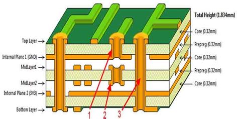
Modern PCBs often consist of multiple layers, each with its own set of traces and vias. An advanced calculator should be capable of handling multi-layer designs and provide accurate trace width recommendations for each layer. This is particularly important for complex designs where signal integrity and thermal management are critical.
Additionally, user-friendly interfaces and integration capabilities with other design tools can greatly enhance the usability of a PCB trace width calculator.
A well-designed interface allows for easy input of parameters and quick access to results, streamlining the design process. Integration with popular PCB design software can further simplify the workflow by enabling seamless data transfer and reducing the likelihood of errors.
Lastly, it is beneficial to have access to detailed documentation and support.
Comprehensive documentation can provide valuable insights into the underlying calculations and assumptions used by the calculator, helping you make informed decisions. Access to technical support can also be invaluable, especially when dealing with complex designs or encountering unexpected issues.
In conclusion, when choosing a PCB trace width calculator, it is crucial to consider features such as current capacity handling, temperature rise calculations, material support, trace configuration options, safety margins, multi-layer capabilities, user-friendly interfaces, integration with design tools, and access to documentation and support. These advanced features can significantly enhance the accuracy and efficiency of your PCB design process, ensuring reliable performance and longevity of the final product.


