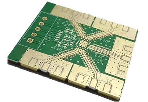
Pcb manufacturing etching
Understanding The Basics Of PCB Etching
Printed Circuit Board (PCB) manufacturing is a complex process that involves several critical steps, one of which is etching. Understanding the basics of PCB etching is essential for anyone involved in electronics design and manufacturing. Etching is a subtractive method used to remove unwanted copper from a copper-clad laminate, leaving behind the desired circuit pattern. This process is fundamental to creating the intricate pathways that allow electronic components to communicate within a device.
Initially, the PCB starts as a flat, rigid sheet of insulating material, typically fiberglass, coated with a thin layer of copper on one or both sides.
The first step in the etching process involves applying a protective mask to the areas of the copper that need to remain intact. This mask can be created using various methods, such as photolithography, where a photosensitive material is applied to the copper surface and then exposed to ultraviolet light through a patterned film. The exposed areas harden, forming a protective barrier, while the unexposed areas remain soft and can be washed away, revealing the copper beneath.
Once the mask is in place, the board is subjected to an etching solution, commonly ferric chloride or ammonium persulfate.
These chemicals react with the exposed copper, dissolving it and leaving behind the masked areas. The choice of etching solution depends on factors such as the desired etching speed, the thickness of the copper layer, and environmental considerations. Ferric chloride, for instance, is widely used due to its effectiveness and relatively low cost, but it requires careful handling and disposal due to its corrosive nature.
During the etching process, it is crucial to maintain consistent agitation and temperature control to ensure uniform removal of the copper.
Inadequate agitation can lead to uneven etching, resulting in defects such as undercutting, where the etchant removes more copper from beneath the mask than intended. Temperature control is equally important, as higher temperatures can accelerate the etching process but may also increase the risk of over-etching, where the etchant penetrates the masked areas.
After the etching is complete, the board is thoroughly rinsed to remove any residual etching solution and then dried.
The protective mask is subsequently stripped away, revealing the final copper traces that form the circuit. At this stage, the board undergoes inspection to ensure that the etching process has produced the desired pattern with the required precision. Any defects identified during this inspection may necessitate rework or, in some cases, scrapping of the board.
In addition to traditional chemical etching, advancements in technology have introduced alternative methods such as laser etching.
Laser etching offers higher precision and can be used to create finer traces, making it suitable for high-density interconnect (HDI) PCBs. However, the cost and complexity of laser etching equipment can be prohibitive for some applications.
Understanding the basics of PCB etching is vital for achieving high-quality circuit boards. The process requires careful attention to detail, from the initial application of the protective mask to the final inspection of the etched board. By mastering these fundamentals, manufacturers can produce reliable and efficient PCBs that meet the stringent demands of modern electronic devices.
Common Chemicals Used In PCB Etching
Printed Circuit Board (PCB) manufacturing is a complex process that involves several stages, one of which is etching. Etching is a critical step in defining the circuit patterns on the board by removing unwanted copper. The chemicals used in this process are pivotal to achieving precision and efficiency. Understanding the common chemicals used in PCB etching can provide valuable insights into the intricacies of this essential manufacturing phase.
One of the most widely used chemicals in PCB etching is ferric chloride (FeCl3).
Ferric chloride is favored for its effectiveness in dissolving copper, making it a popular choice among manufacturers. It is typically used in an aqueous solution, where it reacts with the copper on the PCB to form copper chloride and iron. This reaction is highly efficient, allowing for precise control over the etching process. However, ferric chloride is also known for its corrosive nature, necessitating careful handling and proper disposal to mitigate environmental impact.
Another commonly used etchant is ammonium persulfate ((NH4)2S2O8).
Ammonium persulfate is often chosen for its ability to produce clean and sharp etching results. It works by oxidizing the copper, which then dissolves in the solution. This chemical is particularly advantageous for fine-line etching, where precision is paramount. Despite its benefits, ammonium persulfate requires careful monitoring of concentration and temperature to ensure consistent results. Additionally, it is essential to handle this chemical with care due to its oxidative properties.
Cupric chloride (CuCl2) is also frequently employed in PCB etching.
Cupric chloride offers a unique advantage in that it can be regenerated and reused, making it a more sustainable option compared to other etchants. The regeneration process involves the addition of hydrochloric acid and oxygen, which restores the etching capability of the solution. This not only reduces waste but also lowers operational costs. However, the initial setup for a cupric chloride etching system can be more complex, requiring precise control over the chemical balance and environmental conditions.
Sodium persulfate (Na2S2O8) is another etchant that is gaining popularity in PCB manufacturing.
Similar to ammonium persulfate, sodium persulfate provides excellent etching quality, particularly for high-resolution applications. It operates by oxidizing the copper, which then dissolves in the solution. Sodium persulfate is often preferred for its stability and ease of use. However, like other persulfates, it requires careful handling due to its oxidative nature and potential health hazards.
In addition to these primary etchants, various additives and inhibitors are often used to enhance the etching process.
For instance, surfactants can be added to improve the wetting properties of the etching solution, ensuring uniform contact with the copper surface. Inhibitors may also be used to protect certain areas of the PCB from being etched, allowing for more precise patterning.
The choice of etchant and additives depends on several factors, including the specific requirements of the PCB design, the desired etching quality, and environmental considerations. Each chemical offers distinct advantages and challenges, necessitating a thorough understanding of their properties and interactions.
In conclusion, the chemicals used in PCB etching play a crucial role in defining the final quality and functionality of the circuit board. Ferric chloride, ammonium persulfate, cupric chloride, and sodium persulfate are among the most common etchants, each offering unique benefits and requiring careful handling. By selecting the appropriate chemicals and optimizing their use, manufacturers can achieve precise and efficient etching results, ultimately contributing to the production of high-quality PCBs.

Safety Precautions During PCB Etching
When engaging in the process of PCB manufacturing etching, it is imperative to prioritize safety precautions to mitigate potential hazards. The etching process involves the use of various chemicals, which, if not handled properly, can pose significant risks to both human health and the environment. Therefore, understanding and implementing appropriate safety measures is essential for anyone involved in this intricate procedure.
To begin with, personal protective equipment (PPE) is a fundamental aspect of safety during PCB etching.
Wearing appropriate PPE, such as gloves, safety goggles, and lab coats, is crucial to protect the skin and eyes from corrosive chemicals. Additionally, it is advisable to use a face shield to provide an extra layer of protection against splashes. Ensuring that PPE is made from materials resistant to the chemicals being used is also important to prevent degradation and potential exposure.
Moreover, working in a well-ventilated area is another critical safety measure.
The fumes generated during the etching process can be harmful if inhaled. Therefore, it is recommended to conduct etching in a fume hood or a well-ventilated room equipped with an exhaust system. This helps to dissipate harmful vapors and maintain air quality, thereby reducing the risk of respiratory issues.
In addition to personal protection and ventilation, proper storage and handling of chemicals are paramount.
Chemicals used in PCB etching, such as ferric chloride and ammonium persulfate, should be stored in clearly labeled, corrosion-resistant containers. It is essential to keep these chemicals away from incompatible substances and to store them in a cool, dry place to prevent reactions that could lead to spills or explosions. When handling these chemicals, using tools like chemical-resistant tongs or scoops can further minimize direct contact.
Furthermore, understanding the correct procedures for mixing and disposing of chemicals is vital.
Always follow the manufacturer’s instructions and safety data sheets (SDS) for each chemical. Mixing chemicals in the wrong proportions or combining incompatible substances can result in dangerous reactions. For disposal, it is crucial to adhere to local regulations and guidelines. Improper disposal can lead to environmental contamination and legal repercussions. Many communities offer hazardous waste disposal services, which should be utilized to ensure safe and compliant disposal of etching chemicals.
Another important aspect of safety during PCB etching is emergency preparedness.
Having an emergency plan in place, including access to eyewash stations and safety showers, can make a significant difference in the event of accidental exposure. Additionally, keeping a first aid kit readily available and knowing how to use it can help manage minor injuries effectively. It is also beneficial to have a spill kit on hand to quickly contain and clean up any accidental spills, thereby minimizing exposure and environmental impact.
Lastly, continuous education and training are essential for maintaining a safe working environment.
Regularly updating knowledge on the latest safety protocols and best practices ensures that all individuals involved in PCB etching are well-informed and prepared to handle potential hazards. Conducting periodic safety drills and reviews can reinforce the importance of safety measures and help identify areas for improvement.
In conclusion, safety precautions during PCB manufacturing etching are multifaceted and require diligent attention to detail. By prioritizing personal protective equipment, ensuring proper ventilation, handling and storing chemicals correctly, adhering to disposal regulations, being prepared for emergencies, and committing to ongoing education, the risks associated with PCB etching can be significantly reduced. These measures not only protect individuals but also contribute to a safer and more sustainable manufacturing process.
Troubleshooting Common PCB Etching Issues
Printed Circuit Board (PCB) manufacturing is a complex process that involves several critical steps, one of which is etching. Etching is the process of removing unwanted copper from a PCB to create the desired circuit patterns. Despite its importance, etching can present numerous challenges that can affect the quality and functionality of the final product. Troubleshooting these common PCB etching issues is essential for ensuring the reliability and performance of the circuit boards.
One prevalent issue in PCB etching is under-etching, where insufficient copper is removed, leaving excess material on the board.
This can result from inadequate etchant concentration, insufficient etching time, or low etchant temperature. To address under-etching, it is crucial to ensure that the etchant solution is properly mixed and maintained at the recommended concentration. Additionally, monitoring the etching time and temperature closely can help achieve the desired results. Regular calibration of equipment and adherence to process parameters can significantly reduce the occurrence of under-etching.
Conversely, over-etching is another common problem, where too much copper is removed, potentially damaging the circuit traces and pads.
Over-etching can be caused by excessive etching time, high etchant concentration, or elevated temperatures. To mitigate this issue, it is essential to carefully control the etching duration and maintain the etchant concentration within the specified range. Implementing precise temperature control mechanisms can also help prevent over-etching. Regular inspection of the etched boards can provide early detection of over-etching, allowing for timely adjustments to the process.
Another frequent issue is uneven etching, where the etchant does not remove copper uniformly across the PCB surface.
This can lead to variations in trace widths and potential circuit failures. Uneven etching can result from improper agitation of the etchant solution, inconsistent application of the photoresist, or variations in the PCB material. To troubleshoot uneven etching, it is important to ensure uniform agitation of the etchant solution during the process. Additionally, applying the photoresist evenly and using high-quality PCB materials can help achieve consistent etching results. Regular maintenance and calibration of etching equipment can also contribute to more uniform etching.
Etching defects such as pinholes and voids can also pose significant challenges.
These defects can occur due to contamination on the PCB surface, improper cleaning, or issues with the photoresist application. To address these defects, it is essential to implement thorough cleaning procedures before the etching process. Ensuring a clean and contaminant-free surface can help prevent pinholes and voids. Additionally, using high-quality photoresist materials and applying them uniformly can reduce the likelihood of these defects. Regular inspection and quality control measures can help identify and rectify etching defects early in the process.
Furthermore, etchant disposal and environmental considerations are critical aspects of PCB etching.
Improper disposal of etchant solutions can lead to environmental pollution and regulatory non-compliance. To address this, it is important to follow proper disposal procedures and adhere to environmental regulations. Implementing recycling and waste management practices can help minimize the environmental impact of PCB etching.
In conclusion, troubleshooting common PCB etching issues is essential for ensuring the quality and reliability of printed circuit boards. By addressing under-etching, over-etching, uneven etching, and etching defects, manufacturers can achieve consistent and high-quality results. Additionally, adhering to environmental regulations and implementing proper disposal practices can contribute to sustainable PCB manufacturing. Through careful monitoring, regular maintenance, and adherence to process parameters, manufacturers can effectively troubleshoot and mitigate common etching issues, ensuring the production of reliable and high-performance PCBs.