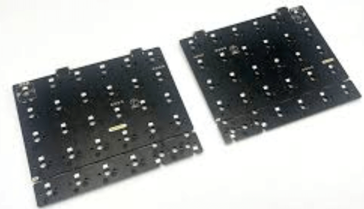
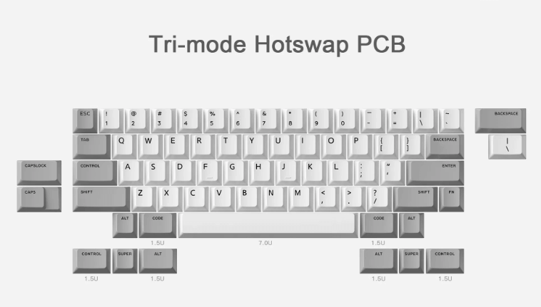
Pcb kit 60
Building Your First Project with the PCB Kit 60: A Step-by-Step Guide
Building your first project with the PCB Kit 60 can be an exciting and rewarding experience, especially for those new to electronics and circuit design. This comprehensive guide aims to provide a clear and structured approach to help you navigate through the process, ensuring that you achieve a successful outcome.
The PCB Kit 60 is designed to offer a versatile platform for various electronic projects, making it an ideal choice for beginners and experienced hobbyists alike.
To begin with, it is essential to familiarize yourself with the components included in the PCB Kit 60.
Typically, the kit contains a printed circuit board (PCB), resistors, capacitors, diodes, transistors, integrated circuits, and various connectors. Additionally, you will find essential tools such as a soldering iron, solder wire, and a multimeter. Understanding the function of each component and tool is crucial, as it will enable you to follow the instructions accurately and troubleshoot any issues that may arise.
Once you have a good grasp of the components, the next step is to plan your project.
Start by selecting a simple circuit design that matches your skill level. Many beginners opt for basic projects such as LED blinkers, simple amplifiers, or basic power supplies. These projects provide a solid foundation for understanding the principles of electronics and circuit design. After selecting your project, gather all the necessary components and tools, and ensure that your workspace is clean and well-organized.
With your project plan in place, it is time to start assembling the circuit.
Begin by placing the components on the PCB according to the schematic diagram provided in the kit. It is important to follow the diagram closely, as incorrect placement can lead to malfunctioning circuits or damage to the components. Use the soldering iron to secure the components to the PCB, ensuring that each connection is clean and free of excess solder. Proper soldering technique is vital for the reliability and longevity of your project.
As you progress through the assembly, periodically check your work using the multimeter.
This tool allows you to measure voltage, current, and resistance, helping you identify any potential issues before they become problematic. For instance, you can use the multimeter to verify that there are no short circuits and that all connections are secure. This step is particularly important for beginners, as it helps build confidence and ensures that the project is on the right track.
After completing the assembly, the next phase involves testing the circuit.
Connect the power supply to the PCB and carefully observe the behavior of the circuit. If the project does not function as expected, refer to the troubleshooting section of the kit’s manual. Common issues include incorrect component placement, poor solder joints, or faulty components. By systematically checking each part of the circuit, you can identify and rectify the problem.
Finally, once your project is functioning correctly, take the time to document your work.
This includes noting any modifications made to the original design, recording test results, and reflecting on the overall experience. Documentation is an invaluable practice, as it allows you to learn from each project and apply that knowledge to future endeavors.
In conclusion, building your first project with the PCB Kit 60 is a structured process that involves careful planning, precise assembly, and thorough testing. By following this step-by-step guide, you can develop a solid understanding of electronics and circuit design, paving the way for more complex and ambitious projects in the future.
Top 5 Tips for Maximizing Efficiency with the PCB Kit 60
The PCB Kit 60 is a versatile and essential tool for electronics enthusiasts and professionals alike. To maximize efficiency when using this kit, it is crucial to adopt certain best practices. By following these top five tips, you can ensure that your projects are not only successful but also completed in a timely and efficient manner.
Firstly, it is important to thoroughly familiarize yourself with the components included in the PCB Kit 60.
This kit typically contains a variety of essential items such as resistors, capacitors, diodes, transistors, and integrated circuits. Taking the time to understand the specifications and functions of each component will enable you to make informed decisions during the design and assembly process. Additionally, organizing these components in a systematic manner can save you valuable time when you need to locate specific parts.
Secondly, proper planning and design are paramount to achieving efficiency.
Before you begin assembling your PCB, it is advisable to create a detailed schematic diagram of your circuit. This diagram serves as a blueprint, guiding you through the placement of components and the routing of connections. Utilizing software tools designed for PCB design can further enhance this process by allowing you to simulate and test your circuit before physically assembling it. This step helps to identify potential issues and make necessary adjustments, thereby reducing the likelihood of errors and rework.
Transitioning to the actual assembly process, the third tip is to ensure that you have the right tools and equipment at your disposal.
High-quality soldering irons, multimeters, and tweezers are indispensable for precise and efficient work. Additionally, using a magnifying glass or microscope can aid in the accurate placement of small components. Investing in these tools not only improves the quality of your work but also speeds up the assembly process by reducing the time spent on troubleshooting and corrections.
Moreover, maintaining a clean and organized workspace is essential for efficiency.
A cluttered work area can lead to misplaced components, accidental damage, and increased assembly time. By keeping your workspace tidy and free of unnecessary items, you can focus more effectively on the task at hand. Implementing a system for managing and storing components, such as labeled containers or drawers, can further streamline your workflow.
Finally, continuous learning and improvement are key to maximizing efficiency with the PCB Kit 60.
The field of electronics is constantly evolving, with new techniques and technologies emerging regularly. Staying updated with the latest advancements and best practices can significantly enhance your skills and efficiency. Participating in online forums, attending workshops, and reading industry publications are excellent ways to stay informed and learn from the experiences of others.
In conclusion, maximizing efficiency with the PCB Kit 60 involves a combination of thorough preparation, proper planning, the right tools, an organized workspace, and a commitment to continuous learning. By implementing these tips, you can ensure that your projects are completed efficiently and to a high standard. Whether you are a hobbyist or a professional, these best practices will help you make the most of your PCB Kit 60 and achieve successful outcomes in your electronic endeavors.
Common Mistakes to Avoid When Using the PCB Kit 60
When working with the PCB Kit 60, it is essential to be aware of common mistakes that can hinder your progress and potentially damage your components. One frequent error is neglecting to thoroughly read the instruction manual before beginning the assembly process. The manual provides crucial information about the specific requirements and steps necessary for successful assembly. Skipping this step can lead to misinterpretation of the instructions, resulting in improper connections and malfunctioning circuits.
Another common mistake is failing to properly organize and inventory the components before starting the project.
The PCB Kit 60 includes numerous small parts, and it is easy to misplace or overlook essential components if they are not systematically arranged. Taking the time to sort and label each part can save significant time and frustration later in the process. Additionally, ensuring that all components are present before beginning can prevent delays caused by missing parts.
Soldering is a critical aspect of working with the PCB Kit 60, and improper soldering techniques can lead to a host of issues.
One prevalent mistake is using excessive heat, which can damage the PCB and the components. It is important to use a soldering iron with a temperature control feature and to apply heat only for the necessary duration. Conversely, insufficient heat can result in cold solder joints, which are unreliable and can cause intermittent connections. Practicing proper soldering techniques, such as using the right amount of solder and ensuring a clean, shiny joint, is essential for the integrity of the circuit.
In addition to soldering, another area where mistakes are commonly made is in the placement of components.
Incorrectly orienting components, such as diodes and capacitors, can prevent the circuit from functioning correctly. Double-checking the orientation and placement of each component against the schematic diagram before soldering can help avoid these errors. Furthermore, it is crucial to ensure that components are seated flush against the PCB to prevent short circuits and ensure a stable connection.
Testing the circuit at various stages of assembly is another practice that can help identify and rectify mistakes early on.
However, a common oversight is neglecting to perform these intermediate tests. By testing the circuit incrementally, you can isolate and address issues as they arise, rather than troubleshooting the entire assembly at the end. This approach can save time and reduce the likelihood of compounded errors.
Another mistake to avoid is overlooking the importance of proper grounding and power supply connections.
Inadequate grounding can lead to noise and instability in the circuit, while incorrect power supply connections can damage components. Ensuring that all ground connections are secure and that the power supply is correctly configured is vital for the reliable operation of the PCB Kit 60.
Finally, it is important to maintain a clean and organized workspace.
A cluttered work area can lead to accidental damage to components and tools, as well as increased risk of static discharge, which can harm sensitive electronic parts. Keeping the workspace tidy and using anti-static measures, such as wrist straps and mats, can help protect your components and ensure a smooth assembly process.
By being mindful of these common mistakes and taking proactive steps to avoid them, you can enhance your experience with the PCB Kit 60 and achieve a successful and reliable assembly.

Advanced Techniques for Customizing Your PCB Kit 60 Projects
The PCB Kit 60 is a versatile and highly customizable tool for electronics enthusiasts and professionals alike. As you delve deeper into your projects, you may find that advanced techniques can significantly enhance the functionality and aesthetics of your custom PCB designs.
One of the first steps in customizing your PCB Kit 60 is to thoroughly understand the layout and components.
By familiarizing yourself with the schematic and the placement of each element, you can make more informed decisions about modifications and enhancements.
Transitioning from basic to advanced customization, consider the importance of component selection.
High-quality components not only improve the performance of your PCB but also ensure longevity and reliability. For instance, opting for low ESR capacitors can reduce noise and improve power efficiency. Similarly, selecting precision resistors can enhance the accuracy of your circuits. As you choose components, keep in mind the specific requirements of your project and the environmental conditions in which your PCB will operate.
Another critical aspect of advanced customization is the optimization of the PCB layout.
Efficient layout design can minimize signal interference and improve overall performance. To achieve this, pay close attention to trace routing. Ensure that high-frequency signals are routed with minimal length and avoid sharp angles, which can cause signal reflection. Additionally, separating analog and digital grounds can reduce noise and improve signal integrity. Utilizing ground planes and power planes can further enhance the stability and performance of your PCB.
Thermal management is another crucial consideration for advanced PCB customization.
As electronic components generate heat, effective thermal management is essential to prevent overheating and ensure reliable operation. Techniques such as adding thermal vias, using heat sinks, and incorporating thermal pads can help dissipate heat more efficiently. Moreover, selecting components with lower power consumption can reduce heat generation and improve the overall efficiency of your design.
Incorporating advanced testing and debugging techniques can also elevate your PCB projects.
Utilizing tools such as oscilloscopes, logic analyzers, and multimeters can help you identify and resolve issues more effectively. Additionally, designing your PCB with test points and debugging interfaces can facilitate easier troubleshooting and iterative improvements. By integrating these advanced testing methods, you can ensure that your PCB functions as intended and meets the desired specifications.
Furthermore, advanced customization often involves the integration of firmware and software.
Developing custom firmware can unlock additional features and functionalities for your PCB. For example, implementing power management algorithms can optimize energy consumption, while custom communication protocols can enhance data transfer efficiency. Collaborating with software developers or learning to code yourself can open up new possibilities for your PCB projects.
Finally, aesthetics and ergonomics should not be overlooked in advanced PCB customization.
A well-designed PCB not only performs well but also looks professional and is easy to use. Consider the placement of connectors, buttons, and LEDs to ensure user-friendly operation. Additionally, using silkscreen layers to label components and provide clear instructions can enhance the usability and maintainability of your PCB.
In conclusion, advanced techniques for customizing your PCB Kit 60 projects encompass a wide range of considerations, from component selection and layout optimization to thermal management, testing, firmware integration, and aesthetics. By applying these advanced techniques, you can create high-performance, reliable, and visually appealing PCBs that meet the specific needs of your projects. As you continue to explore and experiment with these techniques, you will undoubtedly discover new ways to push the boundaries of what your PCB Kit 60 can achieve.