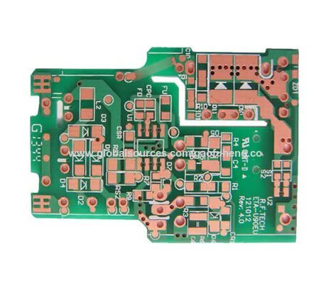
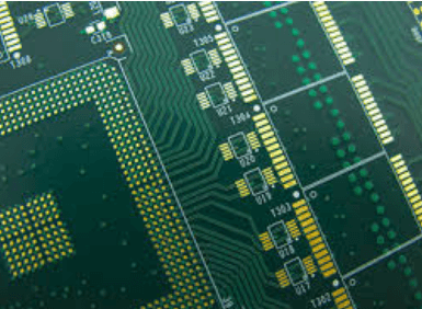
Pcb hdi
Advantages Of PCB HDI In Modern Electronics
High-Density Interconnect (HDI) Printed Circuit Boards (PCBs) have become a cornerstone in the advancement of modern electronics, offering a multitude of advantages that cater to the ever-evolving demands of the industry. As electronic devices continue to shrink in size while increasing in functionality, the need for more efficient and compact circuit boards has never been more critical. HDI PCBs address this need by providing a platform that supports higher component density, improved electrical performance, and enhanced reliability.
One of the primary advantages of HDI PCBs is their ability to accommodate a higher density of components.
This is achieved through the use of microvias, finer lines and spaces, and smaller capture pads, which allow for more components to be placed on a single board. Consequently, this leads to a reduction in the overall size and weight of the electronic device, making HDI PCBs an ideal choice for applications where space is at a premium, such as in smartphones, tablets, and wearable technology. The compact nature of HDI PCBs also contributes to the development of more portable and lightweight devices, which are highly sought after in today’s consumer electronics market.
In addition to their compact size, HDI PCBs offer superior electrical performance compared to traditional PCBs.
The shorter signal paths and reduced parasitic effects in HDI designs result in lower signal loss and faster signal transmission. This is particularly beneficial in high-speed and high-frequency applications, where maintaining signal integrity is crucial. Furthermore, the use of advanced materials and manufacturing techniques in HDI PCBs helps to minimize electromagnetic interference (EMI) and crosstalk, ensuring that the electronic device operates efficiently and reliably.
Another significant advantage of HDI PCBs is their enhanced reliability.
The use of microvias, which are smaller and more robust than traditional vias, reduces the risk of mechanical failure and improves the overall durability of the board. Additionally, the multi-layer construction of HDI PCBs allows for better thermal management, as heat can be dissipated more effectively through the various layers. This is particularly important in high-power applications, where excessive heat can lead to component failure and reduced lifespan of the device. The improved thermal performance of HDI PCBs ensures that electronic devices can operate at optimal temperatures, thereby enhancing their reliability and longevity.
Moreover, HDI PCBs enable greater design flexibility, allowing engineers to create more complex and sophisticated circuits.
The ability to incorporate multiple layers and advanced interconnect techniques provides designers with the freedom to develop innovative solutions that meet the specific requirements of their applications. This flexibility is particularly valuable in industries such as aerospace, automotive, and medical devices, where custom and high-performance solutions are often required.
In conclusion, the advantages of HDI PCBs in modern electronics are manifold. Their ability to support higher component density, improved electrical performance, and enhanced reliability makes them an indispensable component in the development of cutting-edge electronic devices. As the demand for smaller, faster, and more reliable electronics continues to grow, the adoption of HDI PCBs is expected to increase, driving further innovation and progress in the industry. The seamless integration of advanced materials and manufacturing techniques in HDI PCBs ensures that they will remain at the forefront of electronic design, meeting the ever-changing needs of the market.
Design Considerations For HDI PCB Layout
High-Density Interconnect (HDI) Printed Circuit Boards (PCBs) have become increasingly prevalent in modern electronics due to their ability to support complex circuitry within a compact footprint. As the demand for smaller, faster, and more efficient electronic devices continues to grow, the design considerations for HDI PCB layout have become more critical than ever. Understanding these considerations is essential for engineers and designers aiming to optimize performance, reliability, and manufacturability.
One of the primary considerations in HDI PCB design is the selection of materials.
The choice of substrate material can significantly impact the board’s performance, particularly in high-frequency applications. Materials with low dielectric constants and low loss tangents are preferred to minimize signal loss and ensure signal integrity. Additionally, the thermal properties of the substrate must be considered, as HDI PCBs often operate in environments with varying temperatures. Ensuring that the material can withstand thermal cycling without degrading is crucial for long-term reliability.
Another key aspect of HDI PCB design is the layer stack-up configuration.
HDI PCBs typically feature multiple layers, including microvias, buried vias, and blind vias, to achieve high interconnect density. The arrangement of these layers must be carefully planned to optimize signal routing and minimize electromagnetic interference (EMI). Proper layer stack-up can also enhance the board’s mechanical strength and thermal management capabilities. Designers must balance the need for high-density interconnects with the constraints of manufacturability and cost.
Signal integrity is a paramount concern in HDI PCB design.
As signal speeds increase, issues such as crosstalk, impedance mismatches, and signal reflections become more pronounced. To mitigate these issues, designers must employ advanced routing techniques, such as controlled impedance traces and differential pair routing. Additionally, the use of ground planes and power planes can help to reduce noise and provide stable reference voltages. Careful consideration of trace width, spacing, and via placement is essential to maintain signal integrity and ensure reliable operation.
Thermal management is another critical consideration in HDI PCB design.
The high component density and increased power consumption of modern electronic devices can lead to significant heat generation. Effective thermal management strategies, such as the use of thermal vias, heat sinks, and thermal interface materials, are necessary to dissipate heat and prevent overheating. Proper thermal management not only enhances the performance of the device but also extends its lifespan.
Manufacturability is a crucial factor that must be considered throughout the HDI PCB design process.
The complexity of HDI PCBs can pose challenges for fabrication and assembly. Designers must work closely with manufacturers to ensure that the design can be produced using available technologies and processes. This collaboration can help to identify potential issues early in the design phase and avoid costly revisions later. Design for manufacturability (DFM) principles, such as minimizing the use of non-standard components and ensuring adequate spacing for assembly, can facilitate a smoother production process.
In conclusion, the design considerations for HDI PCB layout are multifaceted and require a comprehensive understanding of materials, layer stack-up, signal integrity, thermal management, and manufacturability. By carefully addressing these factors, designers can create HDI PCBs that meet the demanding requirements of modern electronic devices. As technology continues to evolve, staying abreast of advancements in materials, design techniques, and manufacturing processes will be essential for achieving optimal performance and reliability in HDI PCB designs.
Manufacturing Challenges Of HDI PCBs
High-Density Interconnect (HDI) Printed Circuit Boards (PCBs) represent a significant advancement in the field of electronics, offering numerous benefits such as reduced size, increased functionality, and enhanced performance. However, the manufacturing of HDI PCBs presents a unique set of challenges that must be meticulously addressed to ensure the reliability and efficiency of the final product.
One of the primary challenges in HDI PCB manufacturing is the complexity of the design.
HDI PCBs are characterized by their high wiring density, which necessitates the use of finer lines and spaces, smaller vias, and more precise component placement. This increased complexity requires advanced design software and highly skilled engineers to create accurate and functional layouts. The precision needed in the design phase is critical, as any errors can lead to significant issues during manufacturing, potentially resulting in costly rework or even complete redesigns.
Transitioning from design to production, the fabrication process of HDI PCBs involves several sophisticated techniques that are not typically required for standard PCBs.
For instance, the use of microvias, which are much smaller than traditional vias, is a common feature in HDI PCBs. These microvias are often created using laser drilling technology, which demands precise control and calibration to ensure the correct depth and diameter. The accuracy of laser drilling is paramount, as any deviation can compromise the electrical integrity and mechanical stability of the PCB.
Moreover, the lamination process in HDI PCB manufacturing is more intricate compared to conventional PCBs.
HDI PCBs often require multiple lamination cycles to build up the necessary layers, each of which must be perfectly aligned. Misalignment during lamination can lead to defects such as delamination or misregistration, which can severely impact the performance of the PCB. Ensuring proper alignment and adhesion during each lamination cycle is a meticulous task that requires advanced equipment and stringent quality control measures.
Another significant challenge is the selection and handling of materials.
HDI PCBs often utilize advanced materials such as high-performance laminates and specialized copper foils to achieve the desired electrical and thermal properties. These materials can be more sensitive to environmental conditions and handling procedures, necessitating careful storage and processing to prevent contamination or damage. Additionally, the use of these materials can increase the overall cost of the PCB, making cost management a critical aspect of the manufacturing process.
Furthermore, the assembly of HDI PCBs poses its own set of challenges.
The high component density and the use of fine-pitch components require precise placement and soldering techniques. Automated assembly equipment must be capable of handling these small components with high accuracy to avoid defects such as solder bridges or misaligned components. The inspection and testing of HDI PCBs also become more complex due to the increased density and reduced feature sizes, necessitating advanced inspection technologies such as X-ray and automated optical inspection (AOI) systems.
In conclusion, while HDI PCBs offer significant advantages in terms of size, performance, and functionality, their manufacturing process is fraught with challenges that require advanced technology, skilled personnel, and stringent quality control measures. Addressing these challenges effectively is crucial to producing reliable and high-performance HDI PCBs that meet the demanding requirements of modern electronic applications.
Applications Of HDI PCBs In Consumer Electronics
High-Density Interconnect (HDI) Printed Circuit Boards (PCBs) have become a cornerstone in the realm of consumer electronics, driven by the relentless demand for more compact, efficient, and powerful devices. These advanced PCBs are characterized by their higher wiring density per unit area, achieved through finer lines and spaces, smaller vias, and capture pads, as well as higher connection pad density. The applications of HDI PCBs in consumer electronics are vast and varied, reflecting the diverse needs and innovations within the industry.
One of the most prominent applications of HDI PCBs is in smartphones.
Modern smartphones are marvels of miniaturization, packing immense computing power, high-resolution cameras, and a plethora of sensors into a slim form factor. HDI technology enables the integration of these complex functionalities by allowing more components to be placed on both sides of the PCB, connected through microvias. This not only reduces the overall size of the device but also enhances its performance and reliability. The use of HDI PCBs in smartphones is a testament to their ability to support high-speed signal transmission and manage the thermal challenges associated with densely packed electronic components.
In addition to smartphones, HDI PCBs are integral to the design and functionality of tablets and laptops.
These devices require a delicate balance between performance, battery life, and portability. HDI technology facilitates this balance by enabling the incorporation of high-performance processors, memory modules, and other critical components within a limited space. The result is a seamless user experience characterized by fast processing speeds, extended battery life, and sleek designs. Furthermore, the enhanced electrical performance of HDI PCBs ensures that these devices can handle the demands of modern applications, from high-definition video streaming to complex computational tasks.
Wearable technology is another area where HDI PCBs have made a significant impact.
Devices such as smartwatches, fitness trackers, and augmented reality glasses rely on HDI technology to achieve their compact and lightweight designs. The miniaturization capabilities of HDI PCBs allow for the integration of various sensors, communication modules, and power management systems within a small footprint. This not only enhances the functionality of wearable devices but also improves their comfort and usability. As the market for wearable technology continues to grow, the role of HDI PCBs in enabling innovative and user-friendly designs will only become more critical.
Moreover, HDI PCBs are essential in the development of advanced gaming consoles and virtual reality (VR) systems.
These devices demand high processing power and efficient heat dissipation to deliver immersive gaming experiences. HDI technology supports the integration of powerful graphics processors, memory units, and other critical components, ensuring optimal performance and reliability. The ability to manage high-speed signals and reduce electromagnetic interference further enhances the gaming experience, making HDI PCBs a vital component in the evolution of gaming technology.
In conclusion, the applications of HDI PCBs in consumer electronics are extensive and multifaceted, reflecting the diverse and ever-evolving needs of the industry. From smartphones and tablets to wearable technology and gaming consoles, HDI technology enables the creation of compact, efficient, and high-performance devices. As consumer electronics continue to advance, the importance of HDI PCBs in driving innovation and meeting the demands of modern users cannot be overstated. The future of consumer electronics will undoubtedly be shaped by the continued development and application of HDI PCB technology.