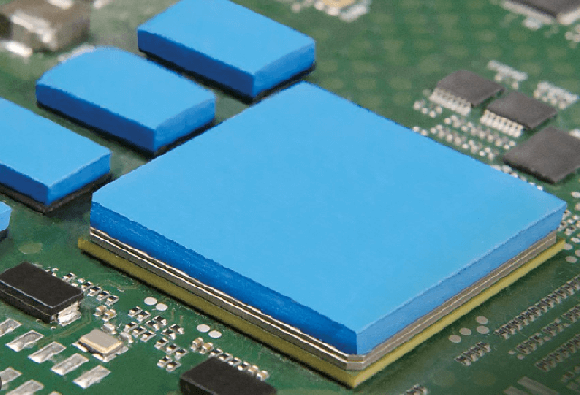
Pcb ground thermal pad
Importance Of Proper Grounding In PCB Thermal Pads
In the realm of printed circuit board (PCB) design, the significance of proper grounding in thermal pads cannot be overstated. Grounding serves as a fundamental aspect that ensures the efficient operation and longevity of electronic devices. The thermal pad, a critical component in PCB design, plays a pivotal role in heat dissipation, which is essential for maintaining the optimal performance of electronic components. Therefore, understanding the importance of proper grounding in PCB thermal pads is crucial for engineers and designers alike.
To begin with, grounding in PCB thermal pads is essential for minimizing electrical noise and interference.
Electrical noise can significantly impact the performance of electronic circuits, leading to erratic behavior and potential malfunction. By providing a low-impedance path to ground, thermal pads help in stabilizing the voltage levels and reducing the susceptibility of the circuit to external electromagnetic interference (EMI). This is particularly important in high-frequency applications where even minor fluctuations can cause substantial disruptions.
Moreover, proper grounding in thermal pads enhances the thermal management of the PCB.
Electronic components generate heat during operation, and if this heat is not effectively dissipated, it can lead to overheating and eventual failure of the components. Thermal pads, when properly grounded, facilitate the efficient transfer of heat away from the components to the ground plane, thereby maintaining a stable operating temperature. This not only prolongs the lifespan of the components but also ensures consistent performance over time.
In addition to thermal management, grounding in PCB thermal pads also contributes to the mechanical stability of the board.
The ground plane acts as a reference point for the entire circuit, providing a stable foundation that helps in mitigating mechanical stresses. This is particularly important in applications where the PCB is subjected to varying environmental conditions, such as temperature fluctuations and mechanical vibrations. A well-grounded thermal pad ensures that the PCB remains structurally sound, thereby preventing potential damage to the components and the board itself.
Furthermore, proper grounding in thermal pads is crucial for ensuring signal integrity.
In high-speed digital circuits, signal integrity is paramount for reliable data transmission. Grounding helps in maintaining a consistent reference voltage, which is essential for accurate signal propagation. Any deviation in the reference voltage can lead to signal distortion and data errors. By providing a stable ground connection, thermal pads help in preserving the integrity of the signals, thereby ensuring reliable communication between different parts of the circuit.
It is also worth noting that proper grounding in PCB thermal pads can aid in compliance with regulatory standards.
Many electronic devices are subject to stringent electromagnetic compatibility (EMC) requirements, which mandate the minimization of EMI emissions. A well-grounded thermal pad helps in achieving these requirements by reducing the overall EMI generated by the circuit. This not only ensures compliance with regulatory standards but also enhances the overall reliability and performance of the device.
In conclusion, the importance of proper grounding in PCB thermal pads cannot be emphasized enough. From minimizing electrical noise and enhancing thermal management to ensuring mechanical stability and signal integrity, grounding plays a vital role in the overall performance and reliability of electronic devices. As such, engineers and designers must pay careful attention to grounding practices in PCB thermal pads to achieve optimal results. By doing so, they can ensure the efficient operation and longevity of their electronic designs, thereby meeting the ever-increasing demands of modern technology.
Techniques For Effective Heat Dissipation Using PCB Ground Thermal Pads
Effective heat dissipation is a critical aspect of electronic circuit design, particularly as devices become more compact and powerful. One of the most efficient methods for managing thermal performance in printed circuit boards (PCBs) is the use of ground thermal pads. These pads serve as a conduit for heat to move away from critical components, thereby enhancing the overall reliability and longevity of the device. Understanding the techniques for effective heat dissipation using PCB ground thermal pads is essential for engineers and designers aiming to optimize their electronic systems.
To begin with, the placement of the ground thermal pad is paramount.
It should be positioned directly beneath the heat-generating component to ensure maximum thermal transfer. This direct contact allows for efficient heat conduction from the component to the PCB. Additionally, the thermal pad should be connected to a large ground plane, which acts as a heat sink, spreading the heat over a larger area and thereby reducing the thermal resistance. This connection is typically achieved through the use of thermal vias, which are small, plated holes that facilitate the transfer of heat from the top layer of the PCB to the internal layers or the bottom layer.
Moreover, the design of the thermal vias is crucial.
The number, size, and distribution of these vias can significantly impact the effectiveness of heat dissipation. A higher number of vias generally improves thermal performance, but it is essential to balance this with the available space and the electrical requirements of the PCB. The diameter of the vias should be optimized to allow for sufficient heat transfer while maintaining structural integrity. Additionally, filling the vias with conductive materials, such as copper, can further enhance thermal conductivity.
Another important consideration is the choice of materials.
The thermal conductivity of the PCB substrate and the solder mask can influence the overall heat dissipation capabilities. High thermal conductivity materials, such as metal-core PCBs or substrates with embedded heat spreaders, can provide superior thermal management compared to traditional FR4 materials. Furthermore, the use of thermal interface materials (TIMs) between the component and the thermal pad can improve the thermal coupling, reducing the thermal resistance and enhancing heat transfer.
In addition to material selection, the layout of the PCB can also affect thermal performance.
Components that generate significant heat should be strategically placed to minimize thermal interference with other sensitive components. Grouping heat-generating components together and placing them near the edge of the PCB can facilitate better heat dissipation. Additionally, ensuring adequate airflow around the PCB can help dissipate heat more effectively. This can be achieved through the use of heat sinks, fans, or other cooling mechanisms.
Furthermore, thermal simulations and modeling can be invaluable tools in the design process.
These techniques allow designers to predict the thermal behavior of the PCB and make informed decisions about the placement of thermal pads, vias, and other heat dissipation features. By simulating different scenarios, designers can optimize the thermal performance of the PCB before physical prototypes are created, saving time and resources.
In conclusion, effective heat dissipation using PCB ground thermal pads involves a combination of strategic placement, optimized via design, appropriate material selection, and thoughtful PCB layout. By considering these factors and utilizing thermal simulations, designers can enhance the thermal performance of their electronic systems, ensuring reliability and longevity. As electronic devices continue to evolve, the importance of efficient thermal management will only increase, making these techniques essential for future innovations.
Common Mistakes To Avoid With PCB Ground Thermal Pads
When designing printed circuit boards (PCBs), the ground thermal pad plays a crucial role in ensuring both electrical performance and thermal management. However, several common mistakes can undermine the effectiveness of these pads, leading to suboptimal performance or even failure of the PCB. Understanding these pitfalls is essential for engineers and designers aiming to optimize their designs.
One frequent mistake is inadequate thermal via placement.
Thermal vias are essential for transferring heat from the thermal pad to other layers of the PCB, thereby dissipating heat more effectively. Insufficient or poorly placed thermal vias can result in localized overheating, which can degrade the performance of components or even cause them to fail. To avoid this, it is important to strategically place an adequate number of thermal vias directly under the thermal pad, ensuring efficient heat transfer.
Another common error is neglecting the solder mask clearance around the thermal pad.
The solder mask is a protective layer that prevents solder from bridging between conductive areas. However, if the solder mask clearance around the thermal pad is too tight, it can impede the flow of solder during the reflow process, leading to poor thermal and electrical connections. Ensuring an appropriate solder mask clearance can facilitate better solder flow and improve the reliability of the thermal pad connection.
Additionally, designers often overlook the importance of proper grounding.
A well-grounded thermal pad can significantly enhance the electrical performance of the PCB by reducing noise and improving signal integrity. However, failing to connect the thermal pad to a solid ground plane can negate these benefits. It is crucial to ensure that the thermal pad is connected to a low-impedance ground plane, which can be achieved by using multiple vias and ensuring a continuous ground path.
Furthermore, improper pad size can also be a significant issue.
If the thermal pad is too small, it may not provide sufficient area for heat dissipation, leading to overheating. Conversely, if the pad is too large, it can cause issues with soldering and may lead to mechanical stress on the component. Therefore, it is essential to follow the component manufacturer’s recommendations for pad size to ensure optimal performance.
Another mistake to avoid is ignoring the impact of thermal relief patterns.
Thermal relief patterns are used to connect the thermal pad to the ground plane while minimizing the risk of thermal stress during soldering. However, if these patterns are not properly designed, they can either impede heat dissipation or cause mechanical issues. It is important to carefully design thermal relief patterns to balance thermal and mechanical considerations.
Lastly, inadequate attention to the overall thermal management of the PCB can render even a well-designed thermal pad ineffective.
This includes considering factors such as airflow, heat sinks, and the placement of heat-generating components. A holistic approach to thermal management ensures that the thermal pad can perform its function effectively within the broader context of the PCB design.
In conclusion, avoiding these common mistakes can significantly enhance the performance and reliability of PCBs with ground thermal pads. By paying careful attention to thermal via placement, solder mask clearance, grounding, pad size, thermal relief patterns, and overall thermal management, designers can ensure that their PCBs operate efficiently and reliably. Understanding and addressing these potential pitfalls is essential for achieving optimal thermal and electrical performance in PCB designs.

Advanced Materials For Enhanced PCB Ground Thermal Pad Performance
In the realm of modern electronics, the performance and reliability of printed circuit boards (PCBs) are paramount. One critical aspect that significantly influences these factors is the PCB ground thermal pad. This component plays a vital role in heat dissipation and electrical grounding, ensuring the stability and longevity of electronic devices. As technology advances, the demand for more efficient and effective thermal management solutions has led to the development of advanced materials specifically designed to enhance the performance of PCB ground thermal pads.
To begin with, traditional materials such as copper and aluminum have been widely used in PCB ground thermal pads due to their excellent thermal conductivity and electrical properties.
However, as electronic devices become more compact and powerful, the limitations of these conventional materials become apparent. Consequently, researchers and engineers have turned their attention to advanced materials that offer superior thermal and electrical performance.
One such material is graphene, a single layer of carbon atoms arranged in a two-dimensional honeycomb lattice.
Graphene exhibits exceptional thermal conductivity, surpassing that of copper by a significant margin. Its unique structure allows for efficient heat transfer, making it an ideal candidate for PCB ground thermal pads. Moreover, graphene’s excellent electrical conductivity ensures effective grounding, further enhancing the overall performance of the PCB. The integration of graphene into thermal pads not only improves heat dissipation but also contributes to the miniaturization of electronic devices, as it allows for thinner and more efficient thermal management solutions.
In addition to graphene, another promising material is boron nitride.
Often referred to as “white graphene,” boron nitride shares many of graphene’s advantageous properties, including high thermal conductivity and electrical insulation. This combination makes boron nitride an excellent choice for applications where electrical isolation is crucial. By incorporating boron nitride into PCB ground thermal pads, engineers can achieve efficient heat dissipation while maintaining electrical isolation, thereby preventing potential short circuits and enhancing device reliability.
Furthermore, the development of composite materials has opened new avenues for enhancing PCB ground thermal pad performance.
These composites typically consist of a polymer matrix embedded with thermally conductive fillers such as ceramic particles or carbon nanotubes. The polymer matrix provides mechanical flexibility and ease of processing, while the fillers significantly boost thermal conductivity. This synergy results in thermal pads that are not only efficient in heat dissipation but also adaptable to various PCB designs and manufacturing processes. The versatility of composite materials allows for tailored solutions that meet the specific thermal management requirements of different electronic devices.
Moreover, phase change materials (PCMs) have emerged as a novel approach to improving thermal management in PCBs.
PCMs absorb and release thermal energy during phase transitions, effectively regulating temperature fluctuations. When integrated into PCB ground thermal pads, PCMs can mitigate temperature spikes and maintain optimal operating conditions for electronic components. This dynamic thermal management capability is particularly beneficial for high-power applications where rapid and efficient heat dissipation is critical.
In conclusion, the quest for enhanced PCB ground thermal pad performance has led to the exploration and development of advanced materials such as graphene, boron nitride, composite materials, and phase change materials. These innovations offer superior thermal and electrical properties, addressing the limitations of traditional materials and meeting the demands of modern electronic devices. As technology continues to evolve, the integration of these advanced materials into PCB ground thermal pads will play a crucial role in ensuring the reliability, efficiency, and longevity of electronic systems.