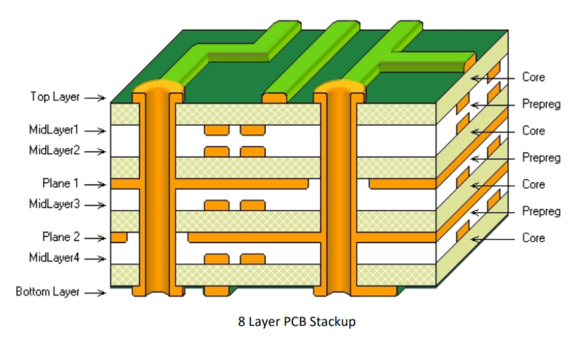
8 layer pcb thickness
Understanding The Importance Of 8 Layer PCB Thickness In Modern Electronics
In the realm of modern electronics, the significance of an 8-layer printed circuit board (PCB) cannot be overstated. As electronic devices become increasingly complex and compact, the demand for multi-layer PCBs has surged. Among these, the 8-layer PCB stands out due to its balance between complexity and manufacturability. Understanding the importance of 8-layer PCB thickness is crucial for engineers and designers aiming to optimize performance, reliability, and cost-effectiveness in their electronic products.
To begin with, the thickness of an 8-layer PCB plays a pivotal role in determining its mechanical strength and durability.
A thicker PCB can better withstand physical stresses, such as bending and vibration, which are common in various applications ranging from consumer electronics to industrial machinery. This robustness is particularly vital in environments where the PCB may be subjected to harsh conditions. Consequently, selecting the appropriate thickness ensures that the PCB maintains its structural integrity over its operational lifespan.
Moreover, the thickness of an 8-layer PCB directly influences its electrical performance.
Thicker PCBs can accommodate wider traces and larger vias, which are essential for managing higher current loads and reducing electrical resistance. This capability is critical in high-power applications where efficient power distribution is paramount. Additionally, the increased thickness can help in minimizing signal loss and crosstalk, thereby enhancing the overall signal integrity. This is especially important in high-frequency applications, such as telecommunications and data processing, where maintaining signal fidelity is crucial.
Transitioning to thermal management, the thickness of an 8-layer PCB also affects its ability to dissipate heat.
Thicker PCBs have a greater capacity to conduct heat away from critical components, thereby preventing overheating and potential damage. Effective thermal management is essential in high-performance electronics, where components generate significant amounts of heat. By optimizing the PCB thickness, designers can ensure that the device operates within safe temperature limits, thereby enhancing reliability and longevity.
Furthermore, the thickness of an 8-layer PCB impacts the manufacturing process and associated costs.
Thicker PCBs require more material and may necessitate additional processing steps, such as extended drilling times for vias. These factors can increase production costs and lead times. However, the benefits of improved performance and reliability often justify these additional expenses. It is essential for designers to strike a balance between the desired electrical and mechanical properties and the economic considerations of manufacturing.
In addition to these technical aspects, the thickness of an 8-layer PCB also has implications for the overall design and layout.
Thicker PCBs provide more space for routing complex circuits, allowing for greater design flexibility. This is particularly advantageous in applications where space is at a premium, and designers need to maximize the functionality within a limited footprint. By carefully selecting the appropriate thickness, designers can achieve a more efficient and compact design without compromising on performance.
In conclusion, the thickness of an 8-layer PCB is a critical parameter that influences various aspects of modern electronics. From mechanical strength and electrical performance to thermal management and manufacturing considerations, the appropriate selection of PCB thickness is essential for optimizing the overall functionality and reliability of electronic devices. As technology continues to advance, the importance of understanding and leveraging the benefits of 8-layer PCB thickness will remain a key factor in the successful development of cutting-edge electronic products.
How 8 Layer PCB Thickness Affects Signal Integrity And Performance
The thickness of an 8-layer printed circuit board (PCB) plays a crucial role in determining its signal integrity and overall performance. As electronic devices become more complex and compact, the demand for multi-layer PCBs has surged, making it essential to understand how the thickness of these layers impacts their functionality.
To begin with, the thickness of an 8-layer PCB is not merely a physical attribute but a critical factor that influences the electrical properties of the board.
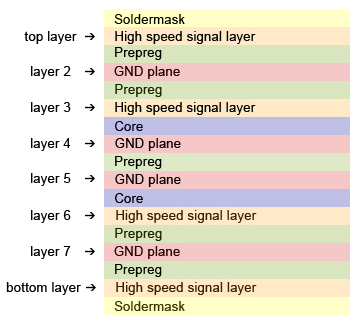
One of the primary considerations is the dielectric constant, which is affected by the thickness of the insulating layers between the conductive layers. A consistent dielectric constant is vital for maintaining signal integrity, as variations can lead to signal distortion and timing issues. Thicker boards tend to have more stable dielectric properties, which can enhance signal transmission and reduce the likelihood of signal loss.
Moreover, the thickness of an 8-layer PCB affects its impedance control.
Impedance matching is essential for high-frequency signal transmission, as mismatched impedance can result in signal reflections and loss. Thicker PCBs allow for better control over the trace width and spacing, which are critical parameters for maintaining the desired impedance levels. This improved control helps in minimizing signal reflections and ensuring that the signals reach their destination with minimal degradation.
In addition to impedance control, the thickness of an 8-layer PCB also impacts its thermal management capabilities.
Thicker boards can dissipate heat more effectively, which is particularly important for high-power applications. Efficient thermal management is crucial for preventing overheating and ensuring the longevity of the electronic components. By providing a more robust thermal pathway, thicker PCBs help in maintaining optimal operating temperatures and enhancing the overall reliability of the device.
Furthermore, the mechanical strength of an 8-layer PCB is directly related to its thickness.
Thicker boards are inherently more rigid, which makes them less susceptible to bending and mechanical stress. This increased rigidity is beneficial for applications that require high durability and resistance to physical damage. However, it is important to strike a balance, as excessively thick boards can be challenging to manufacture and may not be suitable for all applications.
Another aspect to consider is the impact of PCB thickness on signal propagation delay.
Thicker boards can introduce longer signal paths, which may result in increased propagation delay. This delay can be a critical factor in high-speed digital circuits where timing is of the essence. Designers must carefully consider the trade-offs between thickness and signal delay to ensure that the PCB meets the required performance specifications.
Additionally, the thickness of an 8-layer PCB can influence its manufacturability and cost.
Thicker boards may require more advanced fabrication techniques and materials, which can increase production costs. It is essential for designers to weigh the benefits of increased thickness against the potential cost implications to achieve an optimal balance between performance and budget.
In conclusion, the thickness of an 8-layer PCB significantly affects its signal integrity and overall performance. By influencing factors such as dielectric constant, impedance control, thermal management, mechanical strength, signal propagation delay, and manufacturability, the thickness of the PCB plays a pivotal role in determining the success of the final product. Therefore, careful consideration of PCB thickness is essential for achieving the desired performance and reliability in modern electronic devices.
Design Considerations For Optimal 8 Layer PCB Thickness
When designing an 8-layer printed circuit board (PCB), one of the critical factors to consider is the optimal thickness of the board. The thickness of a PCB can significantly impact its performance, reliability, and manufacturability. Therefore, understanding the various design considerations for achieving the ideal thickness is essential for engineers and designers.
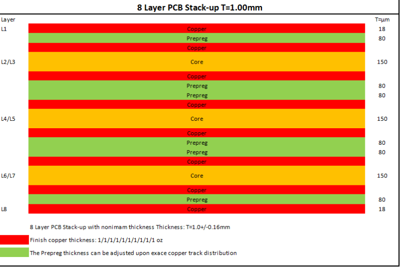
To begin with, the standard thickness for an 8-layer PCB typically ranges from 1.6mm to 2.4mm.
However, the specific thickness can vary depending on the application and the requirements of the end product. One of the primary considerations is the mechanical strength of the PCB. A thicker board generally offers better mechanical stability, which is crucial for applications subjected to physical stress or vibration. Conversely, a thinner board may be more suitable for compact devices where space is at a premium.
Another important factor is the electrical performance of the PCB.
The thickness of the board can influence the impedance of the signal traces, which in turn affects signal integrity. For high-frequency applications, maintaining controlled impedance is vital to minimize signal loss and electromagnetic interference (EMI). Therefore, designers must carefully select the thickness of the dielectric layers between the copper planes to achieve the desired impedance characteristics.
Thermal management is also a key consideration when determining the optimal thickness of an 8-layer PCB.
Thicker boards can dissipate heat more effectively, which is beneficial for high-power applications. However, increased thickness can also lead to higher thermal resistance, potentially causing hotspots and thermal stress. To address this, designers may incorporate thermal vias or use materials with better thermal conductivity to enhance heat dissipation.
Manufacturability is another crucial aspect to consider.
Thicker PCBs can be more challenging to manufacture, as they require more precise drilling and plating processes. Additionally, the increased material usage can lead to higher production costs. Therefore, it is essential to strike a balance between the desired performance characteristics and the practical limitations of the manufacturing process.
Furthermore, the choice of materials plays a significant role in determining the optimal thickness of an 8-layer PCB.
High-quality materials with low dielectric constants and high thermal conductivity can enable thinner boards without compromising performance. However, these materials can be more expensive, so cost considerations must also be taken into account.
In addition to these technical factors, regulatory and industry standards may influence the design decisions.
For instance, certain applications may require compliance with specific standards that dictate minimum or maximum board thickness. Ensuring adherence to these standards is crucial for product certification and market acceptance.
In conclusion, achieving the optimal thickness for an 8-layer PCB involves a careful balance of multiple design considerations. Mechanical strength, electrical performance, thermal management, manufacturability, material selection, and regulatory compliance all play a role in determining the ideal thickness. By thoroughly evaluating these factors, designers can create PCBs that meet the specific requirements of their applications while ensuring reliability and cost-effectiveness. As technology continues to advance, ongoing research and development in materials and manufacturing techniques will further refine the design process, enabling even more precise control over PCB thickness and performance.
Comparing 8 Layer PCB Thickness With Other Multilayer PCB Options
When considering the design and manufacturing of printed circuit boards (PCBs), the number of layers and their corresponding thicknesses play a crucial role in determining the overall performance and application suitability. Among the various multilayer PCB options available, the 8-layer PCB stands out due to its balance between complexity and manageability. To fully appreciate the significance of an 8-layer PCB’s thickness, it is essential to compare it with other multilayer PCB configurations, such as 4-layer, 6-layer, and 10-layer PCBs.
An 8-layer PCB typically has a thickness ranging from 1.2mm to 2.4mm, depending on the specific requirements of the application and the materials used.
This thickness is achieved by stacking multiple layers of conductive and insulating materials, which are then laminated together under high pressure and temperature. The precise control of thickness is vital for ensuring signal integrity, mechanical stability, and thermal management. In comparison, a 4-layer PCB generally has a thickness of around 0.8mm to 1.6mm, while a 6-layer PCB ranges from 1.0mm to 2.0mm. On the other hand, a 10-layer PCB can have a thickness of 1.6mm to 3.2mm or more, depending on the design specifications.
The increased thickness of an 8-layer PCB, as opposed to a 4-layer or 6-layer PCB, provides several advantages.
Firstly, the additional layers allow for more complex routing of signals, which is particularly beneficial for high-density applications such as advanced computing systems, telecommunications equipment, and sophisticated consumer electronics. The extra layers also enable better separation of power and ground planes, which helps in reducing electromagnetic interference (EMI) and improving signal integrity. Furthermore, the increased thickness contributes to enhanced mechanical strength, making the PCB more robust and less prone to warping or bending during assembly and operation.
However, it is important to note that the increased thickness of an 8-layer PCB also presents certain challenges.
For instance, the manufacturing process becomes more intricate, requiring precise control over layer alignment and lamination. This complexity can lead to higher production costs and longer lead times. Additionally, the thicker PCB may pose challenges in terms of heat dissipation, as the increased material volume can impede the efficient transfer of heat away from critical components. Therefore, careful thermal management strategies must be employed to ensure reliable operation.
When comparing an 8-layer PCB to a 10-layer PCB, the differences in thickness and complexity become even more pronounced.
A 10-layer PCB offers even greater routing flexibility and improved signal integrity due to the additional layers. However, this comes at the cost of increased thickness, which can range up to 3.2mm or more. The added complexity of manufacturing a 10-layer PCB further escalates production costs and lead times. Moreover, the thicker PCB may require specialized assembly techniques to accommodate the increased material volume.
In conclusion, the thickness of an 8-layer PCB strikes a balance between the simpler 4-layer and 6-layer configurations and the more complex 10-layer options. While the increased thickness of an 8-layer PCB offers advantages in terms of routing flexibility, signal integrity, and mechanical strength, it also presents challenges related to manufacturing complexity and thermal management. By carefully considering these factors, designers and manufacturers can select the most appropriate multilayer PCB configuration to meet the specific requirements of their applications.