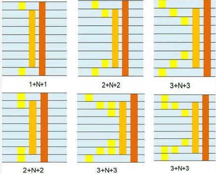
3+n+3 hdi pcb
Advantages Of 3+N+3 HDI PCB In Modern Electronics
The 3+N+3 High-Density Interconnect (HDI) Printed Circuit Board (PCB) has emerged as a pivotal innovation in the realm of modern electronics, offering a multitude of advantages that cater to the ever-evolving demands of the industry. As electronic devices continue to shrink in size while increasing in functionality, the need for more sophisticated and efficient PCB designs has become paramount. The 3+N+3 HDI PCB, characterized by its three sequential layers on both the top and bottom of the core, with an arbitrary number of layers in between, addresses these needs with remarkable efficacy.
One of the foremost advantages of the 3+N+3 HDI PCB is its ability to support higher component density.
This is achieved through the use of microvias, blind vias, and buried vias, which allow for more interconnections within a smaller area. Consequently, designers can incorporate more components and functionalities into a single board without compromising on space. This is particularly beneficial for applications in smartphones, tablets, and other portable devices where space is at a premium. The increased component density also translates to enhanced performance, as signals can travel shorter distances, reducing latency and improving overall speed.
In addition to supporting higher component density, the 3+N+3 HDI PCB offers superior electrical performance.
The use of microvias and other advanced interconnect techniques minimizes signal loss and electromagnetic interference (EMI), which are critical factors in high-speed and high-frequency applications. This results in cleaner signal transmission and improved reliability, making the 3+N+3 HDI PCB an ideal choice for advanced communication systems, high-speed computing, and other performance-critical applications.
Moreover, the 3+N+3 HDI PCB contributes to the overall miniaturization of electronic devices.
By enabling more compact and efficient designs, manufacturers can produce smaller, lighter, and more portable products. This is a significant advantage in the consumer electronics market, where there is a constant demand for sleeker and more aesthetically pleasing devices. The ability to integrate more functionality into a smaller form factor also opens up new possibilities for innovation, allowing designers to explore new features and capabilities that were previously unattainable.
Another notable benefit of the 3+N+3 HDI PCB is its enhanced thermal management capabilities.
The advanced design techniques used in these PCBs facilitate better heat dissipation, which is crucial for maintaining the performance and longevity of electronic components. Effective thermal management is particularly important in high-power applications, where excessive heat can lead to component failure and reduced reliability. By ensuring efficient heat dissipation, the 3+N+3 HDI PCB helps to maintain optimal operating conditions and extend the lifespan of electronic devices.
Furthermore, the 3+N+3 HDI PCB offers greater design flexibility.
The ability to incorporate multiple layers and advanced interconnects allows designers to create more complex and customized PCB layouts. This flexibility is invaluable in meeting the specific requirements of different applications, from consumer electronics to industrial and automotive systems. The versatility of the 3+N+3 HDI PCB also facilitates rapid prototyping and iterative design processes, enabling faster development cycles and quicker time-to-market for new products.
In conclusion, the 3+N+3 HDI PCB stands out as a highly advantageous solution in modern electronics, offering higher component density, superior electrical performance, miniaturization, enhanced thermal management, and greater design flexibility. As the demand for more compact, efficient, and high-performing electronic devices continues to grow, the 3+N+3 HDI PCB is poised to play a crucial role in shaping the future of the industry.
Design Considerations For 3+N+3 HDI PCB
When designing a 3+N+3 High-Density Interconnect (HDI) Printed Circuit Board (PCB), several critical considerations must be taken into account to ensure optimal performance and reliability. The 3+N+3 HDI PCB structure, characterized by three sequential build-up layers on both sides of a core, offers enhanced routing capabilities and higher component density. This complexity necessitates a meticulous approach to design, beginning with material selection.
Material selection is paramount in the design of 3+N+3 HDI PCBs.
The choice of substrate material affects the board’s thermal management, signal integrity, and overall durability. High-frequency applications, for instance, require materials with low dielectric constants and low loss tangents to minimize signal degradation. Additionally, the coefficient of thermal expansion (CTE) must be compatible with the components to prevent mechanical stress during thermal cycling. Therefore, materials such as FR-4, polyimide, and Rogers laminates are often considered based on the specific application requirements.
Transitioning from material selection to layer stack-up design, the arrangement of layers in a 3+N+3 HDI PCB is crucial for achieving the desired electrical performance and manufacturability.
The stack-up must be carefully planned to balance signal layers, power planes, and ground planes. This balance is essential for maintaining signal integrity and reducing electromagnetic interference (EMI). Furthermore, the use of microvias, blind vias, and buried vias in HDI PCBs allows for more efficient interlayer connections, which is particularly beneficial in high-density designs. However, the via structure must be optimized to avoid reliability issues such as via fatigue and to ensure robust electrical connections.
Signal integrity is another critical consideration in the design of 3+N+3 HDI PCBs.
As signal speeds increase, issues such as crosstalk, impedance mismatches, and signal reflections become more pronounced. To mitigate these issues, designers must employ advanced routing techniques, such as controlled impedance routing and differential pair routing. Additionally, the use of ground planes and proper spacing between signal traces can significantly reduce crosstalk and EMI. Signal integrity analysis tools can be invaluable in simulating and validating the design before fabrication.
Thermal management is also a significant concern in 3+N+3 HDI PCB design.
The high component density and increased power consumption can lead to elevated temperatures, which can adversely affect the performance and longevity of the PCB. Effective thermal management strategies include the use of thermal vias, heat sinks, and thermal interface materials. Additionally, the placement of components with high thermal dissipation should be carefully considered to ensure efficient heat distribution and dissipation.
Manufacturability is another aspect that cannot be overlooked.
The complexity of 3+N+3 HDI PCBs requires advanced fabrication techniques and stringent quality control measures. Designers must work closely with manufacturers to ensure that the design can be reliably produced within the capabilities of the fabrication process. This collaboration includes considerations such as minimum trace widths, spacing, and via sizes, as well as the selection of appropriate surface finishes to ensure solderability and long-term reliability.
In conclusion, the design of 3+N+3 HDI PCBs involves a comprehensive approach that encompasses material selection, layer stack-up design, signal integrity, thermal management, and manufacturability. Each of these considerations plays a vital role in ensuring the performance, reliability, and cost-effectiveness of the final product. By meticulously addressing these factors, designers can leverage the advantages of HDI technology to create advanced PCBs that meet the demanding requirements of modern electronic applications.
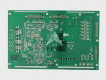
Manufacturing Process Of 3+N+3 HDI PCB
The manufacturing process of a 3+N+3 High-Density Interconnect (HDI) Printed Circuit Board (PCB) is a sophisticated and intricate procedure that demands precision and advanced technology. This type of PCB is characterized by its multiple layers and high interconnect density, which allows for more complex and compact electronic designs. The process begins with the selection of high-quality raw materials, including copper-clad laminates and prepregs, which are essential for ensuring the durability and performance of the final product.
Initially, the inner layers of the PCB are created through a process called inner layer imaging.
This involves coating the copper-clad laminates with a photosensitive material and then exposing them to ultraviolet light through a photomask. The exposed areas are then developed, revealing the desired circuit pattern. Following this, the unwanted copper is etched away, leaving behind the intricate circuitry that forms the foundation of the inner layers. These layers are then subjected to a thorough inspection to ensure that there are no defects or inconsistencies.
Once the inner layers are prepared, they are laminated together using prepregs, which are sheets of fiberglass impregnated with resin.
The lamination process involves stacking the inner layers and prepregs in a specific order and then subjecting them to heat and pressure in a vacuum press. This causes the resin to flow and bond the layers together, forming a solid and cohesive structure. After lamination, the panel is drilled to create vias, which are small holes that allow electrical connections between the different layers of the PCB.
The next step in the manufacturing process is the creation of the outer layers.
Similar to the inner layers, the outer layers are imaged and etched to form the desired circuit patterns. However, in the case of a 3+N+3 HDI PCB, additional microvias are created using laser drilling technology. These microvias are essential for achieving the high interconnect density that characterizes HDI PCBs. The laser drilling process is highly precise and allows for the creation of extremely small and accurately positioned vias.
Following the creation of the outer layers and microvias, the PCB undergoes a series of plating processes.
Electroless copper plating is used to deposit a thin layer of copper on the walls of the vias, ensuring reliable electrical connections between the layers. This is followed by electrolytic copper plating, which builds up the thickness of the copper on the surface of the PCB and within the vias. The plated PCB is then subjected to a series of cleaning and surface preparation steps to ensure that it is free of contaminants and ready for the application of the solder mask.
The solder mask is a protective layer that is applied to the surface of the PCB to prevent solder bridges and short circuits during the assembly process.
It is typically applied using a screen printing or photoimageable process and then cured using ultraviolet light. After the solder mask is applied, the PCB is coated with a surface finish, such as HASL (Hot Air Solder Leveling), ENIG (Electroless Nickel Immersion Gold), or OSP (Organic Solderability Preservative), to protect the exposed copper and ensure good solderability.
Finally, the PCB undergoes a series of electrical tests to verify its functionality and performance. These tests include continuity testing, which checks for open circuits, and isolation testing, which ensures that there are no short circuits between adjacent traces. Once the PCB passes all tests, it is ready for assembly and integration into electronic devices. The manufacturing process of a 3+N+3 HDI PCB is a testament to the advancements in PCB technology and the precision required to meet the demands of modern electronic applications.
Applications Of 3+N+3 HDI PCB In High-Tech Industries
The 3+n+3 High-Density Interconnect (HDI) Printed Circuit Board (PCB) is a sophisticated technology that has found extensive applications in various high-tech industries. This advanced PCB design is characterized by its multiple layers, which include three outer layers on both the top and bottom, and an additional ‘n’ number of inner layers. The intricate structure of 3+n+3 HDI PCBs allows for higher component density, improved electrical performance, and enhanced reliability, making them indispensable in several cutting-edge fields.
One of the primary applications of 3+n+3 HDI PCBs is in the telecommunications industry.
As the demand for faster and more reliable communication networks continues to grow, the need for advanced PCBs that can support high-speed data transmission becomes increasingly critical. 3+n+3 HDI PCBs are particularly well-suited for this purpose due to their ability to accommodate a large number of interconnections within a compact space. This capability is essential for the development of next-generation communication devices, such as 5G smartphones and advanced networking equipment, which require high-speed signal transmission and minimal signal loss.
In addition to telecommunications, the aerospace and defense sectors also benefit significantly from the use of 3+n+3 HDI PCBs.
These industries demand electronic systems that are not only highly reliable but also capable of withstanding extreme environmental conditions. The robust design of 3+n+3 HDI PCBs ensures that they can endure high levels of stress, vibration, and temperature fluctuations, making them ideal for use in critical applications such as avionics, radar systems, and missile guidance systems. Furthermore, the compact nature of these PCBs allows for the miniaturization of electronic components, which is crucial for reducing the overall weight and size of aerospace and defense equipment.
The medical industry is another sector where 3+n+3 HDI PCBs have made a significant impact.
Modern medical devices, such as diagnostic imaging equipment, wearable health monitors, and implantable medical devices, require highly reliable and compact electronic circuits. The advanced design of 3+n+3 HDI PCBs enables the integration of complex functionalities within a small footprint, thereby enhancing the performance and reliability of medical devices. Moreover, the high-density interconnects facilitate the development of more sophisticated and accurate diagnostic tools, ultimately improving patient care and outcomes.
Consumer electronics is yet another domain where the advantages of 3+n+3 HDI PCBs are evident.
The ever-increasing demand for smaller, faster, and more powerful electronic gadgets has driven the need for advanced PCB technologies. 3+n+3 HDI PCBs provide the necessary platform for the development of cutting-edge consumer electronics, such as high-performance laptops, tablets, and gaming consoles. The ability to pack more components into a smaller area not only enhances the functionality of these devices but also contributes to their sleek and compact designs, which are highly sought after by consumers.
In conclusion, the applications of 3+n+3 HDI PCBs in high-tech industries are vast and varied. From telecommunications and aerospace to medical devices and consumer electronics, the advanced design and capabilities of these PCBs have revolutionized the way electronic systems are developed and deployed. As technology continues to evolve, the demand for high-density, high-performance PCBs like the 3+n+3 HDI will only continue to grow, driving further innovation and advancements across multiple industries.