Pcb vs assembly
Differences Between PCB vs Assembly
Printed Circuit Boards (PCBs) are fundamental components in modern electronic devices, serving as the backbone that connects various electronic components. However, the process of creating a functional PCB involves two distinct stages: PCB design and PCB assembly. Understanding the differences between these two stages is crucial for anyone involved in electronics manufacturing or design.
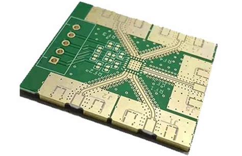
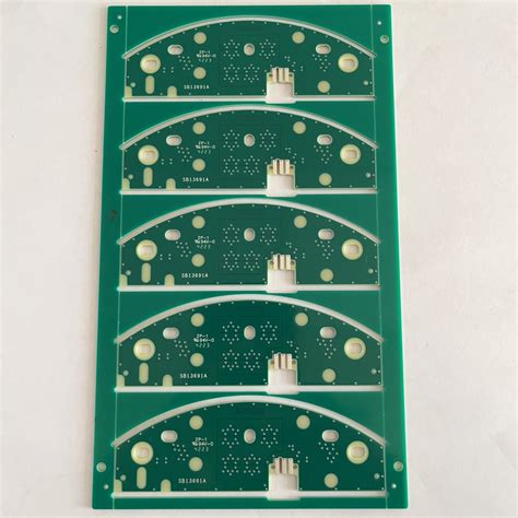
PCB design is the initial phase where the blueprint of the circuit board is created.
This involves a series of steps, starting with schematic capture, where the electronic circuit is drawn using specialized software. Engineers then move on to layout design, where the physical placement of components and routing of electrical connections are meticulously planned. During this stage, considerations such as signal integrity, thermal management, and manufacturability are paramount. The design must comply with industry standards and regulations to ensure reliability and performance. Once the design is finalized, it is converted into Gerber files, which are the standard format used by manufacturers to produce the physical board.
Transitioning from design to assembly, the focus shifts from planning to execution.
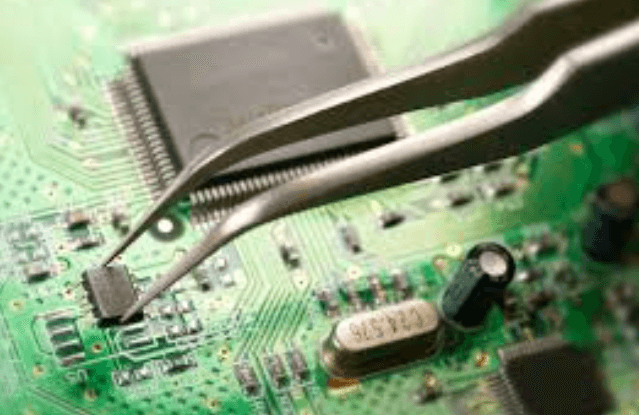
PCB assembly is the process of populating the designed board with electronic components. This stage begins with the procurement of components, which must match the specifications outlined in the design. The assembly process can be divided into several sub-processes, including solder paste application, component placement, soldering, and inspection. Solder paste is first applied to the board using a stencil, ensuring that it is deposited only on the pads where components will be placed. Automated machines then place the components onto the board with high precision.
Following component placement, the board undergoes soldering, which can be done using various methods such as reflow soldering for Surface Mount Technology (SMT) components or wave soldering for Through-Hole Technology (THT) components. Reflow soldering involves passing the board through an oven where the solder paste melts and forms a solid connection between the components and the board. Wave soldering, on the other hand, involves passing the board over a wave of molten solder, which adheres to the exposed metal areas.
After soldering, the assembled board must be inspected to ensure that all components are correctly placed and properly soldered.
This can be done using automated optical inspection (AOI) systems, X-ray inspection, or manual inspection, depending on the complexity and requirements of the board. Any defects identified during inspection must be rectified through rework processes.
While PCB design and PCB assembly are distinct stages, they are interdependent.
A well-designed PCB can simplify the assembly process, reduce costs, and improve the overall reliability of the final product. Conversely, poor design choices can lead to assembly challenges, increased rework, and potential failures in the field. Therefore, effective communication and collaboration between design engineers and assembly technicians are essential to ensure a seamless transition from design to production.
In conclusion, PCB design and PCB assembly are two critical stages in the creation of electronic devices, each with its own set of challenges and requirements. PCB design focuses on creating a detailed blueprint that meets technical and regulatory standards, while PCB assembly involves the practical execution of this blueprint to produce a functional board. Understanding the differences and interdependencies between these stages is key to successful electronics manufacturing.
Key Challenges in PCB Manufacturing vs. PCB Assembly
In the realm of electronics, the processes of PCB manufacturing and PCB assembly are critical yet distinct stages that present unique challenges. Understanding these challenges is essential for ensuring the production of high-quality electronic devices. PCB manufacturing, which involves creating the physical board, and PCB assembly, which entails mounting components onto the board, each have their own set of complexities that must be navigated with precision and expertise.
One of the primary challenges in PCB manufacturing is the intricate design process.
The layout must be meticulously planned to ensure that all components will fit and function correctly. This involves careful consideration of the board’s size, the placement of traces, and the arrangement of layers. Any errors in the design phase can lead to significant issues down the line, such as signal interference or inadequate power distribution. Moreover, the miniaturization of electronic devices has further complicated this process, as designers must now fit more components into smaller spaces without compromising performance.
Transitioning from design to production, the fabrication of the PCB itself presents additional hurdles.
The materials used, such as copper and fiberglass, must be of high quality to ensure durability and reliability. The etching process, which creates the circuit patterns on the board, requires precision to avoid defects like short circuits or open circuits. Furthermore, the drilling of holes for component leads must be accurate to ensure proper alignment and connectivity. Any deviation in these steps can result in a non-functional board, leading to increased costs and delays.
On the other hand, PCB assembly introduces its own set of challenges, starting with the procurement of components.
Ensuring that all components are available and meet the required specifications is a complex task, often complicated by supply chain issues and the need for stringent quality control. Once the components are sourced, the actual assembly process begins, which involves placing and soldering components onto the PCB. This step demands high precision, as even a slight misalignment can affect the performance of the final product.
Surface Mount Technology (SMT) and Through-Hole Technology (THT) are the two primary methods used in PCB assembly.
SMT, which involves placing components directly onto the surface of the board, is favored for its efficiency and suitability for high-density designs. However, it requires advanced machinery and skilled operators to ensure accuracy. THT, which involves inserting component leads through holes in the board and soldering them on the opposite side, is more labor-intensive but provides stronger mechanical bonds, making it ideal for components that will experience physical stress.
Quality control is another critical aspect of both PCB manufacturing and assembly.
In manufacturing, rigorous testing is required to identify any defects in the board before it moves on to assembly. This includes electrical testing to ensure proper connectivity and functionality. In assembly, each solder joint must be inspected to ensure it is free of defects such as cold solder joints or solder bridges. Automated optical inspection (AOI) and X-ray inspection are commonly used to detect these issues, but manual inspection is also necessary for certain components.
In conclusion, while PCB manufacturing and PCB assembly are interconnected processes, each presents its own unique challenges that must be addressed to produce reliable and high-performing electronic devices. From the meticulous design and fabrication of the PCB to the precise placement and soldering of components, every step requires careful attention to detail and a deep understanding of the complexities involved. By navigating these challenges effectively, manufacturers can ensure the production of high-quality PCBs that meet the demands of today’s advanced electronic applications.
Cost Comparison: PCB Fabrication vs. PCB Assembly
When evaluating the costs associated with PCB fabrication and PCB assembly, it is essential to understand the distinct processes involved in each stage and how they contribute to the overall expenditure. PCB fabrication refers to the creation of the bare board, which includes the design, layout, and manufacturing of the physical board itself. On the other hand, PCB assembly involves populating the fabricated board with electronic components to create a functional circuit.
To begin with, the cost of PCB fabrication is influenced by several factors, including the complexity of the board design, the number of layers, the materials used, and the production volume.
Complex designs with multiple layers and intricate layouts require more sophisticated manufacturing techniques and equipment, which can drive up costs. Additionally, the choice of materials, such as high-frequency laminates or specialized substrates, can further impact the price. Production volume also plays a significant role; larger quantities typically benefit from economies of scale, reducing the per-unit cost.
In contrast, PCB assembly costs are primarily driven by the type and number of components, the assembly technology employed, and the labor involved.
Surface mount technology (SMT) and through-hole technology (THT) are the two primary methods used in PCB assembly. SMT is generally more cost-effective for high-volume production due to its automation capabilities, whereas THT may be preferred for specific applications requiring stronger mechanical bonds. The complexity of the assembly process, including the need for precise placement and soldering of components, also affects labor costs. Furthermore, the procurement of components can significantly influence the overall expense, especially if specialized or high-cost components are required.
When comparing the costs of PCB fabrication and PCB assembly, it is crucial to consider the interplay between these stages.
For instance, a highly complex board design may necessitate advanced assembly techniques, thereby increasing the total cost. Conversely, a simpler design may result in lower assembly costs but could still incur higher fabrication expenses if specialized materials are used. Therefore, a holistic approach is necessary to accurately assess the financial implications of both processes.
Moreover, it is important to recognize that the cost structure of PCB fabrication and assembly can vary depending on the geographical location of the manufacturing facilities.
Regions with lower labor costs may offer more competitive pricing for assembly services, while areas with advanced technological infrastructure may provide cost advantages in fabrication. Additionally, the proximity to component suppliers and logistics considerations can further influence the overall cost.
In conclusion, while PCB fabrication and PCB assembly are distinct processes with their own cost determinants, they are intrinsically linked in the production of electronic circuits.
A comprehensive cost comparison must take into account the complexity of the board design, the materials used, the production volume, the type and number of components, and the assembly technology employed. By understanding these factors and their interdependencies, manufacturers can make informed decisions to optimize their production costs and achieve a balance between quality and affordability.
Quality Control in PCB Production vs. PCB Assembly
Quality control is a critical aspect of both PCB production and PCB assembly, ensuring that the final products meet stringent standards and function as intended. In PCB production, quality control begins with the selection of raw materials. High-quality substrates, copper foils, and other materials are essential to produce reliable printed circuit boards.
The manufacturing process involves several stages, including etching, drilling, and plating, each of which requires precise control to maintain the integrity of the board.
Automated optical inspection (AOI) systems are commonly used to detect defects such as misaligned traces, incomplete etching, or surface contamination. These systems provide real-time feedback, allowing for immediate corrective actions and minimizing the risk of defective boards reaching the next stage of production.
Transitioning to the PCB assembly process, quality control takes on a different focus.
Here, the primary concern is the accurate placement and soldering of components onto the PCB. Surface-mount technology (SMT) and through-hole technology (THT) are the two main methods used in assembly, each with its own set of quality control challenges. For SMT, the precision of component placement is crucial, as even slight misalignments can lead to functional failures.
Automated pick-and-place machines are calibrated to ensure components are placed within tight tolerances. Following placement, soldering is performed using reflow ovens, where temperature profiles must be carefully controlled to avoid issues such as cold solder joints or component damage.
In contrast, THT assembly involves inserting components into pre-drilled holes and soldering them on the opposite side of the board.
This method is often used for components that require a stronger mechanical bond. Quality control in THT assembly includes verifying the correct insertion of components and ensuring that solder joints are robust and free of defects. Manual inspection and automated X-ray inspection systems are employed to detect issues that may not be visible to the naked eye, such as internal voids or insufficient solder coverage.
Both PCB production and assembly benefit from rigorous testing protocols to verify functionality and reliability.
Electrical testing, including continuity and isolation tests, is performed to ensure that circuits are correctly formed and that there are no unintended connections. Functional testing, where the assembled PCB is subjected to real-world operating conditions, helps identify any performance issues that may arise during actual use. Environmental stress testing, such as thermal cycling and vibration testing, further ensures that the PCB can withstand the conditions it will encounter in its intended application.
In addition to these technical measures, quality control in both PCB production and assembly involves comprehensive documentation and traceability.
Detailed records of materials, processes, and inspections are maintained to provide a clear history of each board’s production journey. This documentation is invaluable for identifying the root cause of any issues that may arise and for implementing corrective actions to prevent recurrence.
In conclusion, while the focus of quality control differs between PCB production and PCB assembly, both processes are integral to delivering reliable and high-performing electronic products. By employing advanced inspection technologies, rigorous testing protocols, and meticulous documentation practices, manufacturers can ensure that their PCBs meet the highest standards of quality and reliability.