Pcb copper heavy device
Advantages Of Using Heavy Copper In PCB Design
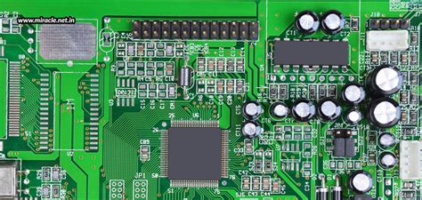
In the realm of printed circuit board (PCB) design, the utilization of heavy copper has garnered significant attention due to its myriad advantages. Heavy copper PCBs, characterized by copper thicknesses exceeding the standard 1 oz/ft², offer enhanced performance and reliability, making them indispensable in various high-power and high-temperature applications. The benefits of incorporating heavy copper into PCB design are multifaceted, encompassing improved thermal management, increased current-carrying capacity, and superior mechanical strength.
One of the foremost advantages of heavy copper in PCB design is its exceptional thermal management capabilities.
In electronic devices, heat dissipation is a critical factor that directly impacts performance and longevity. Heavy copper PCBs excel in this regard by efficiently conducting heat away from critical components, thereby reducing the risk of overheating and thermal damage. This enhanced thermal performance is particularly beneficial in power electronics, automotive, and industrial applications where high power densities are prevalent. By mitigating thermal stress, heavy copper PCBs contribute to the overall reliability and durability of electronic devices.
In addition to superior thermal management, heavy copper PCBs offer a significant increase in current-carrying capacity.
Standard PCBs may struggle to handle high current loads, leading to potential issues such as excessive heat generation and voltage drops. Heavy copper traces, however, can accommodate higher currents without compromising performance. This capability is crucial in applications such as power supplies, motor controllers, and renewable energy systems, where efficient power distribution is paramount. The increased current-carrying capacity of heavy copper PCBs ensures stable and reliable operation, even under demanding conditions.
Moreover, the mechanical strength of heavy copper PCBs is another noteworthy advantage.
The robust construction of these PCBs enhances their resistance to mechanical stresses, such as bending, vibration, and thermal cycling. This durability is essential in environments where electronic devices are subjected to harsh conditions, including aerospace, military, and industrial sectors. The enhanced mechanical strength of heavy copper PCBs not only extends the lifespan of the devices but also reduces the likelihood of failure, thereby ensuring consistent performance over time.
Furthermore, heavy copper PCBs facilitate the integration of complex and compact designs.
The ability to incorporate multiple layers of heavy copper allows for the creation of intricate circuit layouts with high component density. This design flexibility is advantageous in modern electronic devices that demand miniaturization without compromising functionality. By enabling more efficient use of space and resources, heavy copper PCBs support the development of advanced technologies and innovative solutions.
In conclusion, the advantages of using heavy copper in PCB design are substantial and multifaceted.
The superior thermal management, increased current-carrying capacity, and enhanced mechanical strength offered by heavy copper PCBs make them an ideal choice for a wide range of high-power and high-temperature applications. Additionally, the design flexibility afforded by heavy copper PCBs supports the creation of complex and compact electronic devices. As technology continues to evolve, the demand for reliable and efficient PCB solutions will undoubtedly grow, further solidifying the importance of heavy copper in the field of PCB design.
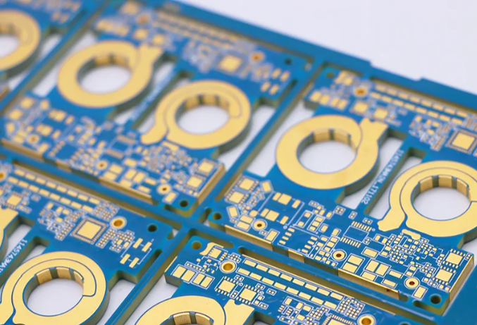
Manufacturing Techniques For Heavy Copper PCBs
Heavy copper PCBs, characterized by their thick copper layers, are essential in applications requiring high current carrying capacity and enhanced thermal management. The manufacturing techniques for these robust circuit boards are more complex than those for standard PCBs, necessitating specialized processes to ensure reliability and performance. Understanding these techniques is crucial for engineers and manufacturers aiming to produce high-quality heavy copper PCBs.
To begin with, the initial step in manufacturing heavy copper PCBs involves selecting the appropriate base material.
Typically, FR4, a glass-reinforced epoxy laminate, is used due to its excellent mechanical and electrical properties. However, for heavy copper applications, the base material must be able to withstand the additional thermal and mechanical stresses imposed by the thick copper layers. Therefore, materials with higher thermal conductivity and stability are often chosen.
Once the base material is selected, the next step is the application of the copper layers.
In standard PCBs, copper layers are usually applied through a process called electroless copper deposition, followed by electroplating. However, for heavy copper PCBs, the copper layers are significantly thicker, often exceeding 3 ounces per square foot. This necessitates a more robust electroplating process, which involves multiple cycles of plating and etching to build up the desired copper thickness. Each cycle must be carefully controlled to ensure uniformity and adhesion of the copper layers.
Following the application of the copper layers, the next critical step is the patterning process.
This involves creating the desired circuit patterns on the copper layers. For heavy copper PCBs, this process is more challenging due to the increased thickness of the copper. Traditional photolithography techniques may not be sufficient, and advanced methods such as laser direct imaging (LDI) are often employed. LDI provides higher precision and accuracy, ensuring that the intricate circuit patterns are accurately transferred onto the thick copper layers.
After patterning, the next step is the etching process, which removes the unwanted copper, leaving behind the desired circuit traces.
For heavy copper PCBs, the etching process must be carefully controlled to prevent undercutting and ensure that the thick copper traces maintain their integrity. This often involves using specialized etching solutions and techniques, such as differential etching, which selectively etches the copper layers at different rates to achieve the desired results.
Once the etching process is complete, the next step is the application of the solder mask.
The solder mask is a protective layer that prevents solder bridges and short circuits during the assembly process. For heavy copper PCBs, the solder mask must be able to adhere to the thick copper layers and withstand the higher thermal stresses. Therefore, specialized solder mask materials and application techniques are often used.
Finally, the last step in the manufacturing process is the application of surface finishes.
Surface finishes protect the exposed copper traces and provide a reliable surface for soldering components. For heavy copper PCBs, surface finishes such as immersion silver, immersion tin, and electroless nickel immersion gold (ENIG) are commonly used due to their excellent conductivity and durability.
In conclusion, the manufacturing techniques for heavy copper PCBs are more complex and demanding than those for standard PCBs. Each step, from material selection to surface finishing, requires careful consideration and specialized processes to ensure the reliability and performance of the final product. By understanding and implementing these techniques, manufacturers can produce high-quality heavy copper PCBs that meet the stringent requirements of high-power and high-reliability applications.
Applications Of Heavy Copper PCBs In High-Power Devices
Heavy copper PCBs, characterized by their thick copper layers, are increasingly becoming indispensable in the realm of high-power devices. These specialized printed circuit boards are designed to handle higher currents and dissipate heat more effectively than their standard counterparts. As a result, they find applications in a variety of high-power devices, where reliability and performance are paramount.
One of the primary applications of heavy copper PCBs is in power supplies.
Power supply units, especially those used in industrial settings, require robust and reliable components to ensure consistent performance. Heavy copper PCBs are ideal for these applications because they can handle high current loads without overheating. The thick copper layers facilitate efficient heat dissipation, thereby enhancing the longevity and reliability of the power supply units. This is particularly crucial in environments where equipment failure can lead to significant downtime and financial losses.
In addition to power supplies, heavy copper PCBs are extensively used in motor controllers.
Motor controllers are essential components in various industries, including automotive, aerospace, and manufacturing. These controllers regulate the speed and torque of electric motors, which are often subjected to high currents. The use of heavy copper PCBs in motor controllers ensures that the circuits can withstand these high currents without degrading. This not only improves the performance of the motor controllers but also extends their operational life, making them more cost-effective in the long run.
Furthermore, heavy copper PCBs are also prevalent in renewable energy systems, such as solar power inverters and wind turbine controllers.
These systems convert and manage the energy generated from renewable sources, which often involves handling high power levels. The robust nature of heavy copper PCBs makes them well-suited for these applications, as they can efficiently manage the high currents and thermal loads associated with energy conversion processes. This contributes to the overall efficiency and reliability of renewable energy systems, which is critical for their widespread adoption and success.
Another significant application of heavy copper PCBs is in electric vehicle (EV) charging stations.
As the demand for electric vehicles continues to rise, the need for efficient and reliable charging infrastructure becomes increasingly important. Heavy copper PCBs play a crucial role in EV charging stations by ensuring that the high currents required for fast charging can be safely and effectively managed. This not only enhances the performance of the charging stations but also ensures the safety of the users, which is a key consideration in the widespread adoption of electric vehicles.
Moreover, heavy copper PCBs are also used in high-power LED lighting systems.
These lighting systems are known for their energy efficiency and long lifespan, but they also generate significant amounts of heat. The thick copper layers in heavy copper PCBs help to dissipate this heat effectively, preventing damage to the LEDs and ensuring consistent performance. This makes heavy copper PCBs an essential component in high-power LED lighting systems, which are increasingly being used in commercial and industrial settings.
In conclusion, the applications of heavy copper PCBs in high-power devices are vast and varied. From power supplies and motor controllers to renewable energy systems and EV charging stations, these specialized PCBs play a critical role in ensuring the reliability and performance of high-power devices. Their ability to handle high currents and dissipate heat effectively makes them indispensable in environments where reliability and performance are paramount. As technology continues to advance, the demand for heavy copper PCBs in high-power applications is only expected to grow, further highlighting their importance in the modern technological landscape.

Thermal Management Solutions With Heavy Copper PCBs
In the realm of modern electronics, thermal management is a critical concern, particularly as devices become more powerful and compact. One of the most effective solutions to this challenge is the use of heavy copper printed circuit boards (PCBs). These specialized PCBs are designed to handle higher currents and dissipate heat more efficiently than their standard counterparts, making them indispensable in high-power applications.
Heavy copper PCBs are characterized by their thicker copper layers, which typically range from 3 ounces per square foot (oz/ft²) to 20 oz/ft² or more.
This increased copper thickness significantly enhances the board’s ability to conduct electricity and manage heat. Consequently, these PCBs are particularly well-suited for applications that demand high power and reliability, such as power supplies, automotive electronics, and industrial control systems.
One of the primary advantages of heavy copper PCBs is their superior thermal management capabilities.
As electronic components generate heat during operation, it is crucial to dissipate this heat effectively to prevent overheating and ensure the longevity of the device. Heavy copper PCBs excel in this regard due to their enhanced thermal conductivity. The thicker copper layers facilitate the efficient transfer of heat away from critical components, thereby reducing the risk of thermal damage and improving overall system performance.
Moreover, heavy copper PCBs offer improved mechanical strength and durability.
The increased copper thickness not only enhances thermal performance but also provides greater structural integrity. This makes heavy copper PCBs more resistant to thermal cycling and mechanical stress, which are common in high-power applications. As a result, devices that utilize heavy copper PCBs tend to have longer lifespans and require less maintenance, translating to cost savings over time.
In addition to their thermal and mechanical benefits, heavy copper PCBs also enable more efficient power distribution.
The thicker copper layers allow for wider and thicker traces, which can carry higher currents without significant voltage drops. This is particularly important in applications where power efficiency is paramount, such as renewable energy systems and electric vehicles. By minimizing power losses and ensuring stable voltage levels, heavy copper PCBs contribute to the overall efficiency and reliability of these systems.
Furthermore, the design flexibility offered by heavy copper PCBs is another noteworthy advantage.
Engineers can incorporate complex and dense circuitry on a single board, thanks to the increased current-carrying capacity and thermal management capabilities. This allows for more compact and efficient designs, which are essential in today’s miniaturized electronic devices. Additionally, heavy copper PCBs can be integrated with other advanced technologies, such as embedded components and multilayer designs, to further enhance their functionality and performance.
Despite their numerous advantages, it is important to note that heavy copper PCBs come with certain challenges.
The manufacturing process for these PCBs is more complex and requires specialized equipment and expertise. This can result in higher production costs compared to standard PCBs. However, the long-term benefits of improved performance, reliability, and durability often outweigh the initial investment, making heavy copper PCBs a worthwhile consideration for high-power applications.
In conclusion, heavy copper PCBs offer a robust solution for thermal management in high-power electronic devices. Their superior thermal conductivity, mechanical strength, and power distribution capabilities make them ideal for a wide range of applications. While the manufacturing process may be more complex and costly, the long-term advantages of using heavy copper PCBs are undeniable. As electronic devices continue to evolve and demand higher performance, the role of heavy copper PCBs in ensuring efficient thermal management and reliable operation will only become more critical.