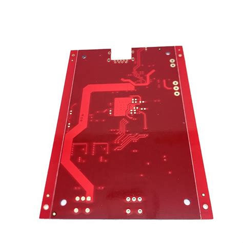
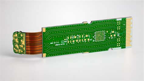
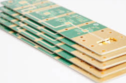
High-speed pcb design for emc and signal integrity
Techniques For Minimizing Crosstalk In High-Speed PCB Design
In high-speed PCB design, minimizing crosstalk is crucial for ensuring electromagnetic compatibility (EMC) and maintaining signal integrity. Crosstalk, the unwanted coupling of signals between adjacent traces, can lead to data corruption, increased noise, and overall system instability. To mitigate these issues, designers must employ a variety of techniques that address the physical layout, grounding, and routing of the PCB.
One effective method for reducing crosstalk is to maintain adequate spacing between signal traces.
By increasing the distance between adjacent traces, the capacitive and inductive coupling that causes crosstalk is significantly reduced. This approach is particularly important for high-speed signals, where even minor interference can have a substantial impact on performance. Additionally, designers should consider the use of differential pairs, which involve routing two complementary signals close together. This technique not only helps to cancel out noise but also minimizes the loop area, further reducing the potential for crosstalk.
Another critical aspect of minimizing crosstalk is the implementation of proper grounding techniques.
A solid ground plane, ideally located directly beneath the signal layers, provides a low-impedance return path for high-frequency signals. This configuration helps to contain electromagnetic fields and reduces the likelihood of crosstalk between traces. Furthermore, designers should ensure that the ground plane is continuous and free of gaps, as discontinuities can disrupt the return path and exacerbate crosstalk issues.
In addition to spacing and grounding, careful routing of signal traces is essential for minimizing crosstalk.
Designers should avoid running high-speed traces in parallel for extended distances, as this increases the likelihood of coupling. Instead, it is advisable to route traces orthogonally between adjacent layers, which helps to break up the parallelism and reduce crosstalk. When parallel routing is unavoidable, incorporating guard traces—grounded traces placed between signal lines—can provide additional isolation and further mitigate crosstalk.
The use of controlled impedance traces is another technique that can help to minimize crosstalk in high-speed PCB design.
By carefully designing the trace width, spacing, and dielectric properties of the PCB material, designers can ensure that the impedance of the traces remains consistent. This consistency helps to maintain signal integrity and reduces the potential for crosstalk. Additionally, controlled impedance traces can be combined with differential pairs to further enhance signal integrity and minimize interference.
Moreover, the strategic placement of decoupling capacitors can play a significant role in reducing crosstalk.
These capacitors help to filter out high-frequency noise and provide a stable power supply to the components on the PCB. By placing decoupling capacitors close to the power pins of integrated circuits, designers can minimize the noise that contributes to crosstalk and improve overall signal integrity.
Finally, the use of simulation and modeling tools can greatly aid in the identification and mitigation of crosstalk issues.
These tools allow designers to analyze the electromagnetic behavior of the PCB and identify potential problem areas before the physical board is manufactured. By simulating different layout configurations and routing strategies, designers can optimize the PCB design to minimize crosstalk and ensure robust performance.
In conclusion, minimizing crosstalk in high-speed PCB design requires a comprehensive approach that includes proper spacing, grounding, routing, controlled impedance, decoupling, and simulation. By employing these techniques, designers can effectively reduce crosstalk, ensuring EMC and maintaining signal integrity in high-speed electronic systems.

Best Practices For Layer Stackup In High-Speed PCB Design
In high-speed PCB design, achieving optimal electromagnetic compatibility (EMC) and signal integrity is paramount. One of the most critical aspects of this process is the layer stackup configuration. Proper layer stackup not only mitigates electromagnetic interference (EMI) but also ensures that signals maintain their integrity as they traverse the PCB. To this end, several best practices should be adhered to when designing the layer stackup for high-speed PCBs.
Firstly, it is essential to understand the role of each layer in the stackup.
Typically, a high-speed PCB will consist of multiple signal layers, power planes, and ground planes. Signal layers are where the actual routing of high-speed signals occurs, while power and ground planes provide the necessary reference and return paths for these signals. A well-designed stackup will strategically place these layers to minimize crosstalk and EMI.
One of the fundamental principles in layer stackup design is to ensure that every signal layer is adjacent to a reference plane, either a ground or power plane.
This proximity helps to contain the electromagnetic fields generated by high-speed signals, thereby reducing EMI. Additionally, having a reference plane close to the signal layer minimizes the loop area for return currents, which is crucial for maintaining signal integrity.
Another best practice is to use a symmetrical stackup.
Symmetry in the layer stackup helps to balance the mechanical stresses during the PCB manufacturing process, reducing the risk of warping and ensuring consistent electrical performance. For instance, if a PCB has four signal layers, it is advisable to place two signal layers on the top half and two on the bottom half, with power and ground planes in between. This balanced approach not only enhances mechanical stability but also improves EMC performance.
Moreover, the placement of power and ground planes should be carefully considered.
It is generally recommended to have a ground plane adjacent to each signal layer. This configuration provides a low-impedance return path for high-speed signals, which is essential for minimizing signal degradation. In cases where a power plane must be adjacent to a signal layer, it is crucial to ensure that the power plane is well-decoupled to act effectively as a reference plane.
The thickness of the dielectric material between layers also plays a significant role in high-speed PCB design.
Thinner dielectrics between signal layers and their adjacent reference planes reduce the loop inductance, which is beneficial for signal integrity. However, it is important to balance this with the need for mechanical strength and manufacturability. Therefore, selecting the appropriate dielectric thickness requires careful consideration of both electrical and mechanical requirements.
Furthermore, the use of multiple ground planes can significantly enhance EMC performance.
Multiple ground planes provide additional shielding and reduce the potential for EMI. When using multiple ground planes, it is advisable to connect them with vias to ensure a low-impedance path for return currents. This practice helps to maintain a consistent reference potential across the PCB, further improving signal integrity.
In conclusion, the layer stackup in high-speed PCB design is a critical factor that influences both EMC and signal integrity. By ensuring that every signal layer is adjacent to a reference plane, using a symmetrical stackup, carefully placing power and ground planes, selecting appropriate dielectric thicknesses, and incorporating multiple ground planes, designers can achieve optimal performance. These best practices, when diligently applied, pave the way for robust and reliable high-speed PCB designs.

Effective Grounding Strategies For EMC Compliance In High-Speed PCBs
Effective grounding strategies are paramount for ensuring electromagnetic compatibility (EMC) and signal integrity in high-speed printed circuit board (PCB) designs. As electronic devices become more complex and operate at higher frequencies, the challenges associated with maintaining EMC compliance and signal integrity intensify. Grounding, a fundamental aspect of PCB design, plays a crucial role in mitigating electromagnetic interference (EMI) and ensuring the reliable operation of high-speed circuits.
One of the primary considerations in grounding strategies is the establishment of a low-impedance ground plane.
A continuous ground plane provides a return path for signals, minimizing the loop area and thereby reducing the potential for radiated emissions. This is particularly important in high-speed designs where signal rise times are fast, and the potential for EMI is significant. By ensuring that the ground plane is uninterrupted, designers can effectively minimize the inductive and capacitive coupling that can lead to signal degradation and EMI issues.
In addition to a continuous ground plane, the concept of ground segregation is essential in high-speed PCB design.
Ground segregation involves separating the ground planes for different functional blocks, such as analog, digital, and power sections. This separation helps to prevent noise from one section from coupling into another, thereby preserving signal integrity. However, it is crucial to carefully manage the connections between these segregated grounds to avoid creating ground loops, which can exacerbate EMI problems. Typically, a single point of connection, often referred to as a star ground, is used to link the segregated grounds, ensuring a controlled and predictable return path for currents.
Another effective grounding strategy is the use of decoupling capacitors.
These capacitors are placed close to the power pins of integrated circuits (ICs) to provide a local reservoir of charge, thereby stabilizing the power supply and reducing noise. Decoupling capacitors help to filter out high-frequency noise and provide a low-impedance path to ground for transient currents. The placement and selection of decoupling capacitors are critical; they should be positioned as close as possible to the ICs and chosen based on their frequency response characteristics to ensure optimal performance.
Via stitching is also a valuable technique in high-speed PCB design for enhancing grounding.
By placing vias at regular intervals along the ground plane, designers can create a more robust and low-impedance connection between different layers of the PCB. This helps to maintain signal integrity by providing a consistent return path for high-frequency signals and reducing the potential for EMI. Via stitching is particularly important in multilayer PCBs, where signals may traverse multiple layers, and maintaining a continuous ground path is essential.
Furthermore, careful routing of high-speed signals is necessary to complement effective grounding strategies.
Differential pairs, for instance, should be routed with consistent spacing and minimal skew to ensure that the signals remain balanced and immune to common-mode noise. Additionally, signal traces should be kept as short as possible and routed over a continuous ground plane to minimize the loop area and reduce the potential for radiated emissions.
In conclusion, effective grounding strategies are critical for achieving EMC compliance and maintaining signal integrity in high-speed PCB designs. By implementing a continuous ground plane, segregating grounds, using decoupling capacitors, employing via stitching, and carefully routing high-speed signals, designers can mitigate EMI issues and ensure the reliable operation of their circuits. As electronic devices continue to evolve and operate at higher frequencies, the importance of robust grounding strategies cannot be overstated.

Signal Integrity Analysis Tools And Methods For High-Speed PCB Design
In the realm of high-speed PCB design, ensuring signal integrity is paramount to achieving optimal performance and reliability. Signal integrity refers to the quality and fidelity of electrical signals as they traverse through the PCB, and it is influenced by various factors such as signal reflections, crosstalk, and electromagnetic interference (EMI). To address these challenges, designers employ a range of signal integrity analysis tools and methods that facilitate the identification and mitigation of potential issues early in the design process.
One of the primary tools used in signal integrity analysis is simulation software.
These sophisticated programs allow designers to model the behavior of electrical signals within the PCB layout, providing insights into how signals will propagate through different traces and components. By simulating the PCB design, engineers can predict potential signal integrity problems such as reflections caused by impedance mismatches or signal degradation due to excessive trace length. This predictive capability is crucial for making informed design decisions and implementing corrective measures before physical prototypes are manufactured.
In addition to simulation software, time-domain reflectometry (TDR) is another valuable method for analyzing signal integrity.
TDR involves sending a fast-rise-time pulse down a transmission line and observing the reflections that occur due to impedance discontinuities. By examining the reflected signals, designers can pinpoint the locations and magnitudes of impedance mismatches, which are often the culprits behind signal reflections and subsequent data corruption. TDR provides a direct and practical approach to diagnosing and addressing signal integrity issues in high-speed PCB designs.
Moreover, the use of eye diagrams is a common technique for assessing signal integrity in high-speed digital circuits.
An eye diagram is a graphical representation of a digital signal’s voltage over time, superimposed over multiple cycles. The resulting “eye” pattern provides a visual indication of the signal’s quality, with a wide-open eye suggesting good signal integrity and a closed or distorted eye indicating potential problems. Eye diagrams are particularly useful for evaluating the effects of jitter, noise, and other impairments on high-speed signals, enabling designers to make necessary adjustments to improve performance.
Furthermore, crosstalk analysis is essential for maintaining signal integrity in densely packed PCBs.
Crosstalk occurs when a signal in one trace induces unwanted noise in an adjacent trace, potentially leading to data errors and signal degradation. To mitigate crosstalk, designers can use simulation tools to analyze the coupling between traces and implement strategies such as increasing trace spacing, using differential signaling, or incorporating ground planes to shield sensitive signals. By proactively addressing crosstalk, designers can ensure that high-speed signals remain clean and reliable.
Additionally, electromagnetic compatibility (EMC) considerations play a critical role in signal integrity analysis.
High-speed PCBs are susceptible to EMI, which can disrupt signal transmission and degrade performance. To combat EMI, designers can use tools such as electromagnetic field solvers to model and analyze the PCB’s electromagnetic environment. These tools help identify potential sources of EMI and guide the implementation of design practices such as proper grounding, shielding, and filtering to minimize electromagnetic interference and enhance signal integrity.
In conclusion, signal integrity analysis tools and methods are indispensable for high-speed PCB design. By leveraging simulation software, time-domain reflectometry, eye diagrams, crosstalk analysis, and EMC considerations, designers can proactively identify and mitigate potential signal integrity issues. These techniques enable the creation of robust and reliable high-speed PCBs that meet the stringent performance requirements of modern electronic systems. As technology continues to advance, the importance of signal integrity analysis in high-speed PCB design will only grow, underscoring the need for designers to stay abreast of the latest tools and methodologies in this critical field.


