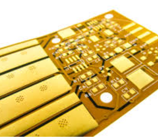
Best 6 layer pcb stackup
Understanding the Basics: Why a 6 Layer PCB Stackup Matters
In the realm of electronics design, the printed circuit board (PCB) serves as the backbone of most electronic devices, providing the necessary support and connectivity for electronic components. As technology advances, the complexity of these boards has increased, leading to the development of multi-layer PCBs. Among these, the 6-layer PCB stackup has emerged as a popular choice for many applications, offering a balance between performance, cost, and design flexibility. Understanding why a 6-layer PCB stackup matters requires an exploration of its structure, benefits, and applications.
To begin with, a 6-layer PCB stackup consists of six layers of conductive material, typically copper, separated by insulating layers.
This configuration allows for more intricate routing of electrical signals compared to simpler designs, such as single or double-layer PCBs. The additional layers provide more space for routing, which is particularly beneficial in complex circuits where signal integrity and electromagnetic interference (EMI) are of concern. By strategically arranging the layers, designers can optimize the board for specific electrical characteristics, such as impedance control and signal isolation.
Moreover, the 6-layer stackup offers significant advantages in terms of signal integrity.
With more layers available, designers can dedicate specific layers to power and ground planes, which help in reducing noise and crosstalk between signal traces. This is crucial in high-speed digital circuits where maintaining signal integrity is paramount. The presence of dedicated power and ground planes also aids in the distribution of power across the board, ensuring that all components receive stable and consistent power, thereby enhancing the overall reliability of the device.
In addition to signal integrity, the 6-layer PCB stackup is advantageous for thermal management.
As electronic devices become more powerful, they generate more heat, which can affect performance and longevity. The additional layers in a 6-layer PCB can be used to dissipate heat more effectively, either by incorporating thermal vias or by using specific materials with better thermal conductivity. This capability is particularly important in applications such as telecommunications, computing, and automotive electronics, where devices are often subjected to high thermal loads.
Furthermore, the 6-layer PCB stackup provides a cost-effective solution for many applications.
While it is more expensive than simpler PCBs, it offers a good compromise between cost and performance. The additional layers allow for more compact designs, which can reduce the overall size and weight of the device. This is particularly beneficial in portable electronics, where space is at a premium. Additionally, the improved performance and reliability can lead to cost savings in the long run by reducing the need for additional components or design iterations.
In conclusion, the 6-layer PCB stackup is a critical component in modern electronics design, offering a range of benefits that make it an attractive choice for many applications. Its ability to enhance signal integrity, improve thermal management, and provide a cost-effective solution makes it a versatile option for designers. As technology continues to evolve, the importance of understanding and utilizing multi-layer PCB stackups, such as the 6-layer configuration, will only grow, underscoring their significance in the development of advanced electronic devices.
Design Tips for Optimal Performance in 6 Layer PCB Stackups
When designing a six-layer printed circuit board (PCB), achieving optimal performance requires careful consideration of the stackup configuration. A well-planned stackup not only enhances the electrical performance but also improves the mechanical stability and manufacturability of the PCB. To begin with, understanding the fundamental purpose of each layer in a six-layer PCB is crucial. Typically, these layers include two outer layers for components and routing, two inner signal layers, and two internal planes for power and ground. This configuration provides a balanced approach to managing signal integrity, power distribution, and electromagnetic interference (EMI).
One of the primary considerations in designing a six-layer PCB stackup is the arrangement of signal and plane layers.
A common and effective configuration is to place the power and ground planes adjacent to each other in the middle of the stackup. This arrangement creates a low-inductance path for power distribution, which is essential for minimizing voltage fluctuations and ensuring stable power delivery to all components. Additionally, having the power and ground planes closely coupled helps in reducing EMI by providing a return path for high-frequency signals, thereby minimizing loop areas.
Transitioning to the signal layers, it is advisable to sandwich them between the power and ground planes.
This setup not only shields the signal layers from external noise but also enhances signal integrity by providing a controlled impedance environment. Controlled impedance is critical for high-speed digital signals, as it reduces signal reflections and crosstalk, which can degrade the performance of the PCB. Moreover, by placing the signal layers between the planes, designers can achieve better isolation between different signal traces, further reducing the risk of interference.
Another important aspect to consider is the thickness of the dielectric material between the layers.
The dielectric thickness influences the characteristic impedance of the signal traces, which must be carefully controlled to match the impedance requirements of the components and connectors used in the design. By selecting the appropriate dielectric material and thickness, designers can fine-tune the impedance and ensure that the PCB meets the desired electrical specifications.
Furthermore, the choice of materials plays a significant role in the overall performance of the PCB.
High-quality materials with low dielectric constant and low loss tangent are preferred for high-frequency applications, as they minimize signal attenuation and dispersion. Additionally, using materials with good thermal properties can enhance the thermal management of the PCB, which is particularly important in applications with high power density.
In addition to electrical considerations, mechanical factors such as board thickness and layer symmetry should not be overlooked.
A balanced stackup with symmetrical layer distribution helps prevent warping and bowing during the manufacturing process, ensuring that the PCB maintains its structural integrity. This is especially important for boards that will undergo multiple thermal cycles during assembly and operation.
In conclusion, designing a six-layer PCB stackup for optimal performance involves a careful balance of electrical, mechanical, and material considerations. By strategically arranging the signal and plane layers, selecting appropriate materials, and ensuring controlled impedance, designers can create a PCB that meets the demanding requirements of modern electronic applications. As technology continues to advance, the importance of a well-designed PCB stackup becomes even more critical, underscoring the need for meticulous planning and attention to detail in the design process.

Common Mistakes to Avoid in 6 Layer PCB Stackup Design
Designing a 6-layer PCB stackup is a complex task that requires careful consideration of various factors to ensure optimal performance and reliability. However, even experienced designers can fall into common pitfalls that may compromise the functionality of the final product.
One of the most frequent mistakes is neglecting the importance of proper layer arrangement.
The sequence in which the layers are stacked plays a crucial role in signal integrity and electromagnetic compatibility. For instance, placing power and ground planes adjacent to each other can significantly reduce electromagnetic interference, a factor often overlooked in the rush to meet design deadlines.
Another common error is the inadequate allocation of ground planes.
Ground planes are essential for providing a return path for signals and minimizing noise. Designers sometimes underestimate the number of ground planes needed, leading to increased signal interference and potential circuit failure. It is advisable to dedicate at least one layer entirely to ground, ensuring a stable reference point for all signals. Furthermore, the placement of signal layers should be carefully considered. Signals should ideally be routed between two planes, such as a power and a ground plane, to create a controlled impedance environment. This arrangement helps in maintaining signal integrity and reducing crosstalk between adjacent traces.
Transitioning to the topic of trace width and spacing, it is crucial to adhere to the design rules specified for the PCB material being used.
Designers often make the mistake of using uniform trace widths and spacings across all layers, disregarding the specific requirements of high-speed signals. High-speed traces require careful impedance matching, which can be achieved by adjusting trace widths and spacings according to the dielectric properties of the materials. Failure to do so can result in signal reflections and loss, severely affecting the performance of the PCB.
Thermal management is another aspect that is frequently underestimated in 6-layer PCB designs.
With multiple layers, heat dissipation becomes a challenge, and improper thermal management can lead to overheating and component failure. Designers should incorporate thermal vias and consider the use of thermal reliefs to facilitate heat dissipation. Additionally, the placement of heat-generating components should be strategically planned to avoid hotspots and ensure even heat distribution across the board.
Moving on to the aspect of via design, vias are often improperly implemented, leading to increased parasitic inductance and capacitance.
Blind and buried vias can be beneficial in saving space and reducing signal path lengths, but they must be used judiciously. Overuse of vias can complicate the manufacturing process and increase costs. It is essential to balance the use of vias with the overall design requirements, ensuring that they do not compromise signal integrity.
Lastly, documentation and communication with the manufacturing team are critical yet frequently overlooked aspects of PCB design.
Incomplete or unclear documentation can lead to manufacturing errors, resulting in costly revisions and delays. Designers should ensure that all design files are thoroughly reviewed and that clear instructions are provided to the manufacturer. This includes specifying material types, layer stackup details, and any special requirements for the PCB.
In conclusion, avoiding these common mistakes in 6-layer PCB stackup design requires a comprehensive understanding of the principles of signal integrity, thermal management, and manufacturing processes. By paying attention to these details and maintaining clear communication with the manufacturing team, designers can create efficient and reliable PCBs that meet the desired performance criteria.
Innovative Applications of 6 Layer PCB Stackups in Modern Electronics
In the rapidly evolving landscape of modern electronics, the demand for more compact, efficient, and high-performance devices has led to significant advancements in printed circuit board (PCB) technology. Among these advancements, the 6-layer PCB stackup has emerged as a versatile and innovative solution, offering a balance between complexity and cost-effectiveness. This configuration is increasingly being utilized in a variety of applications, from consumer electronics to industrial machinery, due to its ability to enhance electrical performance while maintaining manageable production costs.
To understand the innovative applications of 6-layer PCB stackups, it is essential to first consider their structural advantages.
A 6-layer PCB typically consists of two outer layers and four inner layers, which can be strategically arranged to optimize signal integrity, power distribution, and electromagnetic interference (EMI) shielding. This configuration allows for the separation of signal layers and power planes, reducing crosstalk and improving overall circuit performance. Consequently, these attributes make 6-layer PCBs particularly suitable for applications requiring high-speed data transmission and precise signal processing.
One of the most prominent applications of 6-layer PCB stackups is in the realm of consumer electronics, where devices such as smartphones, tablets, and laptops demand compact designs without compromising functionality.
The additional layers in a 6-layer PCB provide the necessary real estate for routing complex circuits, accommodating more components, and integrating advanced features like wireless connectivity and high-resolution displays. Moreover, the enhanced thermal management capabilities of 6-layer PCBs are crucial in preventing overheating in densely packed electronic devices, thereby ensuring reliability and longevity.
In addition to consumer electronics, the automotive industry has also embraced 6-layer PCB stackups for their ability to support the sophisticated electronic systems found in modern vehicles.
As cars become increasingly reliant on electronic control units (ECUs) for functions ranging from engine management to advanced driver-assistance systems (ADAS), the need for robust and efficient PCBs has grown. The 6-layer configuration allows for the integration of multiple functionalities within a single board, reducing weight and space while maintaining the high performance required for automotive applications.
Furthermore, the telecommunications sector benefits significantly from the use of 6-layer PCBs, particularly in the development of networking equipment and infrastructure.
As the demand for faster and more reliable internet connectivity continues to rise, the need for PCBs that can handle high-frequency signals and large data volumes becomes paramount. The 6-layer stackup provides the necessary signal integrity and EMI shielding to support these requirements, making it an ideal choice for routers, switches, and other communication devices.
In the realm of industrial electronics, 6-layer PCBs are employed in the design of complex machinery and control systems.
These applications often require PCBs that can withstand harsh environments and operate reliably under demanding conditions. The additional layers in a 6-layer stackup can be used to incorporate protective features such as ground planes and thermal vias, enhancing the board’s durability and performance.
In conclusion, the innovative applications of 6-layer PCB stackups in modern electronics are vast and varied, driven by their ability to meet the demands of high-performance, compact, and reliable electronic devices. As technology continues to advance, the role of 6-layer PCBs in enabling these innovations will undoubtedly expand, solidifying their place as a cornerstone of modern electronic design.