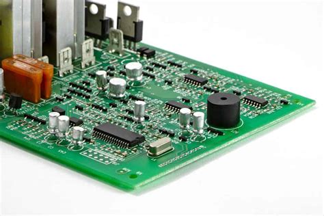
Pcb prototype assembly
Benefits Of Rapid PCB Prototype Assembly In Product Development
In the fast-paced world of product development, the ability to quickly and efficiently bring ideas to life is paramount.
One of the most critical components in the development of electronic products is the printed circuit board (PCB).
The process of PCB prototype assembly plays a crucial role in this context, offering numerous benefits that significantly enhance the product development cycle. By understanding these advantages, companies can better leverage this technology to maintain a competitive edge.
To begin with, rapid PCB prototype assembly allows for accelerated testing and validation of design concepts.
In traditional product development cycles, the time taken to move from design to production can be extensive, often leading to delays and increased costs. However, with rapid prototyping, designers can quickly create functional models of their PCBs, enabling them to test and refine their designs in a fraction of the time. This swift turnaround is particularly beneficial in industries where time-to-market is a critical factor, such as consumer electronics and telecommunications.
Moreover, rapid PCB prototype assembly facilitates iterative design processes.
In the early stages of product development, it is common for designs to undergo multiple revisions. Each iteration provides an opportunity to identify and rectify potential issues, ensuring that the final product meets the desired specifications and quality standards. By enabling quick and cost-effective production of prototypes, rapid PCB assembly supports this iterative approach, allowing designers to experiment with different configurations and components without incurring significant expenses.
In addition to speeding up the design process, rapid PCB prototype assembly also enhances communication and collaboration among development teams.
When engineers and designers have access to physical prototypes, they can more effectively convey their ideas and insights to colleagues and stakeholders. This tangible representation of the design fosters a clearer understanding of the product’s functionality and potential challenges, leading to more informed decision-making and a more cohesive development process.
Furthermore, the use of rapid PCB prototype assembly can lead to significant cost savings.
Traditional methods of PCB production often involve high setup costs and minimum order quantities, which can be prohibitive for small-scale projects or startups. In contrast, rapid prototyping services typically offer lower setup costs and the flexibility to produce small batches, making it an economically viable option for companies of all sizes. This cost-effectiveness allows businesses to allocate resources more efficiently, investing in other critical areas of product development such as marketing and distribution.
Another notable benefit of rapid PCB prototype assembly is the ability to incorporate cutting-edge technologies and materials into the design.
As the electronics industry continues to evolve, new components and materials are constantly being developed. Rapid prototyping enables designers to experiment with these innovations, integrating them into their designs to create more advanced and competitive products. This adaptability is essential in a market where consumer expectations are continually rising, and technological advancements are frequent.
In conclusion, the benefits of rapid PCB prototype assembly in product development are manifold. By accelerating the testing and validation process, supporting iterative design, enhancing communication, reducing costs, and enabling the integration of new technologies, this approach significantly contributes to the efficiency and success of product development efforts. As companies strive to innovate and deliver high-quality products to market, embracing rapid PCB prototype assembly will undoubtedly remain a key strategy in achieving these goals.
Key Challenges In PCB Prototype Assembly And How To Overcome Them
Printed Circuit Board (PCB) prototype assembly is a critical phase in the development of electronic devices, serving as a bridge between design and mass production. However, this stage is fraught with challenges that can impede progress and affect the final product’s quality. Understanding these challenges and implementing strategies to overcome them is essential for successful PCB prototype assembly.
One of the primary challenges in PCB prototype assembly is the complexity of modern electronic designs.
As devices become more sophisticated, the PCBs that support them must accommodate a higher density of components and intricate circuitry. This complexity can lead to design errors, which, if not identified early, can result in costly rework or even complete redesigns. To mitigate this risk, it is crucial to employ advanced design software that offers simulation and validation tools. These tools can help identify potential issues before the physical assembly begins, thereby saving time and resources.
Another significant challenge is the selection of appropriate materials and components.
The choice of materials can greatly influence the performance and reliability of the PCB. For instance, selecting the wrong substrate material can lead to issues such as signal loss or thermal instability. Similarly, using components that are not compatible with the design specifications can result in functional failures. To address this, it is advisable to work closely with suppliers and manufacturers to ensure that the materials and components meet the required standards and specifications. Additionally, maintaining a comprehensive database of approved components can streamline the selection process and reduce the likelihood of errors.
The assembly process itself presents its own set of challenges, particularly in terms of precision and accuracy.
As PCBs become smaller and more densely packed, the margin for error in placing components diminishes. Automated assembly equipment, such as pick-and-place machines, can enhance precision, but they must be properly calibrated and maintained to function effectively. Regular maintenance and calibration of assembly equipment are essential to ensure that components are placed accurately and that soldering is performed correctly. Furthermore, implementing rigorous quality control measures, such as automated optical inspection (AOI) and X-ray inspection, can help detect assembly defects early in the process.
Time constraints also pose a significant challenge in PCB prototype assembly.
The pressure to bring products to market quickly can lead to rushed processes, increasing the likelihood of errors. To overcome this, it is important to establish a realistic timeline that allows for thorough testing and validation at each stage of the assembly process. Agile project management techniques can be beneficial in this regard, as they promote iterative development and continuous feedback, enabling teams to identify and address issues promptly.
Finally, communication and collaboration among the various stakeholders involved in PCB prototype assembly are crucial.
Miscommunication between design engineers, manufacturers, and suppliers can lead to misunderstandings and errors. Establishing clear communication channels and fostering a collaborative environment can help ensure that everyone is aligned and working towards the same goals. Regular meetings and updates can facilitate this process, allowing for the timely exchange of information and the resolution of any issues that may arise.
In conclusion, while PCB prototype assembly presents several challenges, they can be effectively managed through careful planning, the use of advanced tools and technologies, and fostering strong collaboration among stakeholders. By addressing these challenges proactively, organizations can enhance the quality and reliability of their PCBs, ultimately leading to more successful electronic products.
Innovations In PCB Prototype Assembly Technology
In recent years, the field of PCB prototype assembly has witnessed significant innovations, driven by the relentless pursuit of efficiency, precision, and miniaturization. As electronic devices become increasingly complex and compact, the demand for advanced PCB prototype assembly technologies has surged. This evolution is not only reshaping the electronics manufacturing landscape but also setting new standards for quality and performance.
One of the most notable advancements in PCB prototype assembly is the integration of automated processes.
Automation has revolutionized the way PCBs are assembled, significantly reducing human error and increasing production speed. Automated pick-and-place machines, for instance, have become indispensable in modern assembly lines. These machines are capable of placing thousands of components per hour with remarkable accuracy, ensuring that even the most intricate designs are executed flawlessly. Moreover, automation facilitates rapid prototyping, allowing engineers to iterate designs quickly and efficiently, thus accelerating the product development cycle.
In addition to automation, the advent of surface mount technology (SMT) has been a game-changer in PCB prototype assembly.
SMT allows components to be mounted directly onto the surface of the PCB, eliminating the need for through-hole components and enabling more compact and lightweight designs. This technology not only enhances the electrical performance of the circuit but also reduces manufacturing costs by minimizing material usage and assembly time. As a result, SMT has become the preferred method for assembling PCBs in a wide range of applications, from consumer electronics to aerospace systems.
Furthermore, the use of advanced materials in PCB prototype assembly has opened new avenues for innovation.
High-performance substrates, such as polyimide and ceramic, offer superior thermal and electrical properties compared to traditional materials like FR-4. These advanced substrates are particularly beneficial in applications that require high reliability and performance under extreme conditions, such as automotive and military electronics. By leveraging these materials, manufacturers can produce PCBs that are not only more durable but also capable of supporting higher frequencies and power levels.
Another significant development in PCB prototype assembly is the implementation of advanced inspection and testing techniques.
As PCBs become more complex, ensuring their quality and reliability is paramount. Innovations such as automated optical inspection (AOI) and X-ray inspection have become integral to the assembly process. These technologies enable manufacturers to detect defects and inconsistencies at various stages of production, ensuring that only flawless products reach the market. Additionally, functional testing methods have evolved to accommodate the growing complexity of electronic circuits, providing comprehensive validation of PCB performance before deployment.
Moreover, the rise of digital twin technology is poised to further transform PCB prototype assembly.
By creating a virtual replica of the physical PCB, engineers can simulate and analyze the assembly process in a digital environment. This approach allows for the identification and resolution of potential issues before they occur in the real world, thereby reducing the risk of costly errors and rework. Digital twins also facilitate collaboration among design, manufacturing, and testing teams, fostering a more integrated and efficient development process.
In conclusion, the innovations in PCB prototype assembly technology are driving the electronics industry toward new heights of efficiency and capability. Through automation, advanced materials, cutting-edge inspection techniques, and digital twin technology, manufacturers are able to meet the ever-increasing demands for high-performance, reliable, and compact electronic devices. As these technologies continue to evolve, they will undoubtedly pave the way for even more groundbreaking advancements in the future.
Best Practices For Efficient PCB Prototype Assembly
In the realm of electronics manufacturing, the process of PCB prototype assembly is a critical step that bridges the gap between design and mass production. To ensure efficiency and success in this phase, it is essential to adhere to a set of best practices that can streamline operations and minimize potential errors. By focusing on these practices, manufacturers can enhance the quality and reliability of their prototypes, ultimately leading to a smoother transition to full-scale production.
To begin with, meticulous planning is paramount.
Before embarking on the assembly process, it is crucial to have a comprehensive understanding of the design specifications and requirements. This involves a thorough review of the schematic diagrams and bill of materials (BOM) to ensure that all components are accurately listed and available. By doing so, manufacturers can prevent delays caused by missing or incorrect parts, thereby maintaining the momentum of the assembly process.
Furthermore, effective communication between the design and assembly teams cannot be overstated. .
Establishing a clear line of communication ensures that any ambiguities or discrepancies in the design are promptly addressed. This collaborative approach not only fosters a better understanding of the project but also facilitates the identification of potential issues before they escalate into costly mistakes. Regular meetings and updates can serve as a platform for discussing progress and challenges, thereby promoting a proactive problem-solving environment.
In addition to planning and communication, the selection of appropriate tools and equipment plays a significant role in the efficiency of PCB prototype assembly.
Investing in high-quality soldering stations, pick-and-place machines, and inspection tools can significantly enhance the precision and speed of the assembly process. Moreover, the use of automated equipment can reduce the likelihood of human error, leading to more consistent and reliable outcomes. It is also advisable to keep abreast of technological advancements in assembly equipment, as these innovations can offer new opportunities for improving efficiency.
Another critical aspect of efficient PCB prototype assembly is the implementation of rigorous quality control measures.
Conducting thorough inspections at various stages of the assembly process can help identify defects early on, allowing for timely corrective actions. Techniques such as automated optical inspection (AOI) and X-ray inspection can be employed to detect issues that may not be visible to the naked eye. By maintaining a high standard of quality control, manufacturers can ensure that the final product meets the desired specifications and performance criteria.
Moreover, the importance of documentation should not be overlooked.
Keeping detailed records of the assembly process, including any modifications or deviations from the original design, can provide valuable insights for future projects. This documentation serves as a reference point for troubleshooting and can aid in refining assembly techniques over time. Additionally, it can facilitate knowledge transfer within the organization, ensuring that best practices are consistently applied across different projects.
In conclusion, efficient PCB prototype assembly is a multifaceted endeavor that requires careful planning, effective communication, the right tools, stringent quality control, and thorough documentation. By adhering to these best practices, manufacturers can optimize their assembly processes, reduce the risk of errors, and ultimately produce high-quality prototypes that pave the way for successful mass production. As the electronics industry continues to evolve, staying committed to these principles will be essential for maintaining a competitive edge and delivering innovative solutions to the market.