Press hole rogers pcb
Understanding the Role of Press-Fit Holes in Rogers PCB Design
In the realm of printed circuit board (PCB) design, the integration of press-fit holes has emerged as a pivotal technique, particularly when working with Rogers materials. These materials, known for their superior high-frequency performance, are often employed in applications such as telecommunications, aerospace, and advanced computing. Understanding the role of press-fit holes in Rogers PCB design is essential for engineers and designers aiming to optimize the functionality and reliability of their electronic devices.
Press-fit technology offers a solderless method of connecting components to a PCB, which is particularly advantageous in high-frequency applications where thermal and mechanical stresses can compromise solder joints.
. The press-fit process involves inserting a component pin into a precisely sized hole on the PCB, where the pin is held in place by friction. This method not only enhances mechanical stability but also ensures excellent electrical connectivity, which is crucial for maintaining signal integrity in high-frequency circuits.
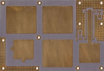
Rogers PCBs, known for their low dielectric loss and stable dielectric constant, are often used in environments where signal integrity is paramount.
The integration of press-fit holes in these PCBs can significantly enhance their performance by providing robust connections that withstand environmental stresses. Moreover, the absence of solder in press-fit connections eliminates the risk of thermal damage to the Rogers material, which can occur during the soldering process. This is particularly important given the sensitivity of Rogers materials to high temperatures.
Furthermore, the use of press-fit holes in Rogers PCB design can lead to improved manufacturing efficiency.
The elimination of the soldering process reduces production time and costs, while also minimizing the potential for defects associated with soldering, such as cold joints or bridging. This efficiency is particularly beneficial in high-volume production environments where time and cost savings are critical.
In addition to these practical benefits, press-fit technology also offers design flexibility.
Engineers can design PCBs with higher component densities without the constraints imposed by soldering. This flexibility is especially valuable in applications where space is limited, and the demand for miniaturization is high. By allowing for more compact and efficient designs, press-fit holes enable the development of advanced electronic devices that meet the ever-evolving demands of modern technology.
However, the successful implementation of press-fit holes in Rogers PCB design requires careful consideration of several factors.
The precision of hole dimensions is critical, as any deviation can compromise the integrity of the connection. Additionally, the choice of press-fit pin material and design must be compatible with the specific Rogers material used to ensure optimal performance. Engineers must also consider the potential impact of environmental factors, such as temperature fluctuations and mechanical vibrations, on the long-term reliability of press-fit connections.
In conclusion, the integration of press-fit holes in Rogers PCB design offers numerous advantages, from enhanced mechanical and electrical performance to improved manufacturing efficiency and design flexibility. As the demand for high-frequency applications continues to grow, the role of press-fit technology in Rogers PCBs is likely to become increasingly significant. By understanding and leveraging the benefits of press-fit holes, engineers can develop innovative solutions that meet the challenges of modern electronic design.
Advantages of Using Press-Fit Technology in Rogers PCBs
Press-fit technology has emerged as a significant advancement in the field of printed circuit boards (PCBs), particularly when applied to Rogers PCBs. This innovative approach offers numerous advantages that enhance the performance, reliability, and manufacturability of electronic devices. To begin with, one of the primary benefits of using press-fit technology in Rogers PCBs is the elimination of soldering processes. Traditional soldering can introduce thermal stress and potential defects, such as cold solder joints or bridging, which can compromise the integrity of the connection. By contrast, press-fit technology relies on mechanical force to establish a secure and reliable connection, thereby reducing the risk of such defects and enhancing the overall durability of the PCB.
Moreover, press-fit technology contributes to improved electrical performance.
The press-fit connection provides a low-resistance path, which is crucial for high-frequency applications where signal integrity is paramount. Rogers PCBs, known for their excellent dielectric properties and low signal loss, are often used in high-frequency and microwave applications. The combination of Rogers materials with press-fit technology ensures that the electrical performance is optimized, making it an ideal choice for applications that demand high-speed data transmission and minimal signal distortion.
In addition to electrical performance, press-fit technology offers significant advantages in terms of assembly and rework processes.
The absence of soldering simplifies the assembly process, as it eliminates the need for solder paste application, reflow ovens, and cleaning processes associated with traditional soldering. This not only reduces manufacturing time and costs but also minimizes the environmental impact by eliminating the use of flux and other chemicals. Furthermore, press-fit connections are reversible, allowing for easy rework and repair. Components can be removed and replaced without damaging the PCB, which is particularly beneficial in prototyping and testing phases where design changes are frequent.
Another noteworthy advantage of press-fit technology in Rogers PCBs is its compatibility with high-density interconnect (HDI) designs.
As electronic devices become increasingly compact and complex, the demand for HDI PCBs has grown. Press-fit technology supports this trend by enabling reliable connections in densely packed circuits without the need for additional space for solder pads. This allows for more efficient use of the PCB real estate, facilitating the design of smaller and more powerful electronic devices.
Furthermore, the mechanical robustness of press-fit connections enhances the reliability of Rogers PCBs in harsh environments.
The mechanical retention provided by press-fit technology ensures that connections remain stable under conditions of vibration, shock, and thermal cycling. This makes it particularly suitable for applications in the automotive, aerospace, and industrial sectors, where reliability and durability are critical.
In conclusion, the integration of press-fit technology in Rogers PCBs offers a multitude of advantages that cater to the evolving demands of modern electronic applications. By eliminating soldering, enhancing electrical performance, simplifying assembly and rework, supporting HDI designs, and providing mechanical robustness, press-fit technology stands out as a superior choice for engineers and manufacturers seeking to optimize the performance and reliability of their electronic devices. As the electronics industry continues to advance, the adoption of press-fit technology in Rogers PCBs is likely to become increasingly prevalent, driving innovation and efficiency in PCB design and manufacturing.
Step-by-Step Guide to Implementing Press Holes in Rogers PCBs
Implementing press holes in Rogers PCBs is a meticulous process that requires a comprehensive understanding of both the material properties and the technical requirements of the circuit board design. Rogers PCBs, known for their superior performance in high-frequency applications, demand precision and attention to detail, especially when integrating press holes. This guide aims to provide a step-by-step approach to effectively incorporate press holes into Rogers PCBs, ensuring optimal functionality and reliability.
To begin with, it is essential to understand the purpose of press holes in PCB design.
Press holes, often referred to as vias, are used to establish electrical connections between different layers of a multilayer PCB. In Rogers PCBs, which are frequently used in RF and microwave applications, these connections must be precise to maintain signal integrity. Therefore, the first step in implementing press holes is to carefully plan the PCB layout. This involves determining the exact locations where the press holes will be placed, taking into account the electrical pathways and the overall design of the circuit.
Once the layout is finalized, the next step is to select the appropriate tools and materials.
Rogers PCBs are made from high-frequency laminates, which require specialized drilling equipment to create clean and accurate holes. It is crucial to use drill bits that are specifically designed for these materials to prevent any damage or deformation. Additionally, selecting the right size and type of press hole is vital. The diameter of the hole must be compatible with the components and the intended electrical connections, ensuring a snug fit that will not compromise the board’s performance.
After selecting the tools and materials, the drilling process can commence.
This step demands precision and control, as any deviation can lead to misalignment or damage to the PCB. It is advisable to use automated drilling machines that offer high accuracy and repeatability. During drilling, maintaining a clean environment is essential to prevent any debris from affecting the quality of the holes. Once the holes are drilled, they must be thoroughly cleaned to remove any residual material that could interfere with the electrical connections.
Following the drilling and cleaning process, the next step is to insert the press-fit components into the holes.
This requires careful handling to avoid damaging the delicate Rogers material. The components should be aligned precisely with the holes and pressed in using a controlled force to ensure a secure fit. It is important to verify that each component is properly seated and that there are no gaps or misalignments that could affect the board’s performance.
Finally, after all the press-fit components are installed, the PCB should undergo a series of tests to ensure its functionality and reliability.
These tests typically include electrical continuity checks, impedance measurements, and thermal cycling tests to simulate real-world operating conditions. Any issues identified during testing should be addressed promptly to prevent potential failures in the field.
In conclusion, implementing press holes in Rogers PCBs is a complex process that requires careful planning, precise execution, and thorough testing. By following these steps, designers and manufacturers can ensure that their PCBs meet the high standards required for high-frequency applications, ultimately leading to more reliable and efficient electronic devices.
Common Challenges and Solutions in Press Hole Rogers PCB Manufacturing
In the realm of printed circuit board (PCB) manufacturing, the use of Rogers materials has become increasingly prevalent due to their superior performance in high-frequency applications. However, the process of creating press hole Rogers PCBs presents a unique set of challenges that manufacturers must navigate to ensure optimal functionality and reliability. Understanding these challenges and implementing effective solutions is crucial for achieving high-quality outcomes.
One of the primary challenges in press hole Rogers PCB manufacturing is the material’s inherent properties.
Rogers materials, known for their excellent dielectric properties and thermal stability, are also characterized by their softness and flexibility. This can lead to difficulties during the drilling process, as the material may deform or delaminate, resulting in inaccurate hole sizes or compromised structural integrity. To address this issue, manufacturers often employ specialized drilling techniques and equipment. Utilizing sharp, high-quality drill bits and optimizing drilling parameters such as speed and feed rate can significantly reduce the risk of material deformation and ensure precise hole dimensions.
Another significant challenge is the adhesion of copper layers to the Rogers substrate.
The unique surface characteristics of Rogers materials can hinder the bonding process, leading to potential delamination during thermal cycling or mechanical stress. To mitigate this, manufacturers typically employ surface treatment techniques such as plasma etching or chemical roughening to enhance the adhesion properties of the substrate. Additionally, selecting appropriate bonding materials and optimizing lamination processes can further improve the reliability of copper layer adhesion.
Thermal management is also a critical consideration in press hole Rogers PCB manufacturing.
The high-frequency applications for which these PCBs are often used generate significant heat, which can adversely affect performance and longevity. Effective thermal management solutions are essential to dissipate heat and maintain optimal operating temperatures. This can be achieved through the incorporation of thermal vias, heat sinks, or advanced cooling techniques. By carefully designing the PCB layout and selecting materials with high thermal conductivity, manufacturers can enhance heat dissipation and ensure the long-term reliability of the PCB.
Moreover, the precision required in the registration and alignment of multilayer Rogers PCBs poses another challenge.
Misalignment during the lamination process can lead to signal integrity issues and compromised electrical performance. To overcome this, manufacturers employ advanced alignment systems and inspection techniques to ensure precise layer registration. Automated optical inspection (AOI) and X-ray inspection are commonly used to verify alignment accuracy and detect any potential defects early in the manufacturing process.
Finally, the cost implications of using Rogers materials cannot be overlooked.
While they offer superior performance, Rogers materials are generally more expensive than traditional FR-4 substrates. This necessitates careful cost management and optimization strategies to ensure that the benefits of using Rogers materials outweigh the additional expenses. Manufacturers often focus on process optimization, waste reduction, and efficient material utilization to minimize costs without compromising quality.
In conclusion, the manufacturing of press hole Rogers PCBs involves navigating a series of complex challenges, from material properties and adhesion issues to thermal management and alignment precision. By employing specialized techniques, advanced equipment, and rigorous inspection processes, manufacturers can effectively address these challenges and produce high-performance PCBs that meet the demanding requirements of modern electronic applications. Through continuous innovation and process refinement, the industry can continue to advance, ensuring that Rogers PCBs remain a cornerstone of high-frequency electronic design.