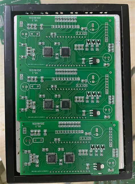
Rf filter pcb layout
Importance Of Grounding In RF Filter PCB Layout
In the realm of radio frequency (RF) design, the importance of grounding in RF filter printed circuit board (PCB) layout cannot be overstated. Grounding serves as the foundation upon which the performance and reliability of RF circuits are built. As RF filters are integral components in communication systems, ensuring their optimal functionality is paramount. Proper grounding techniques are essential to minimize noise, reduce electromagnetic interference (EMI), and enhance signal integrity, thereby ensuring that the RF filter performs its intended function effectively.
To begin with, grounding in RF filter PCB layout is crucial for minimizing noise.
Noise, which can originate from various sources such as power supplies, digital circuits, or external electromagnetic fields, can significantly degrade the performance of RF filters. By implementing a well-designed grounding scheme, designers can create a low-impedance path for noise to dissipate, thereby preventing it from coupling into sensitive RF circuits. This is particularly important in RF applications where even minor noise can lead to significant signal distortion or loss of data integrity.
Moreover, effective grounding is instrumental in reducing electromagnetic interference.
EMI is a common challenge in RF design, as it can originate from both internal and external sources. Internally, components on the PCB can generate electromagnetic fields that interfere with each other, while externally, RF circuits can be susceptible to interference from nearby electronic devices. A robust grounding strategy helps to shield the RF filter from these unwanted electromagnetic fields. By providing a continuous ground plane, designers can create a Faraday cage effect, which effectively isolates the RF filter from external EMI sources. This not only protects the filter but also prevents it from emitting interference that could affect other components or systems.
In addition to noise reduction and EMI mitigation, grounding plays a pivotal role in enhancing signal integrity.
Signal integrity refers to the preservation of the quality and fidelity of the signal as it travels through the RF filter. Poor grounding can lead to issues such as signal reflection, crosstalk, and impedance mismatches, all of which can degrade signal integrity. By ensuring a solid and continuous ground connection, designers can maintain consistent impedance levels across the PCB, thereby minimizing signal reflections and ensuring that the signal remains intact as it passes through the filter.
Furthermore, grounding is essential for thermal management in RF filter PCB layouts.
RF circuits can generate significant amounts of heat, which, if not properly managed, can lead to component failure or reduced performance. A well-designed ground plane can act as a heat sink, dissipating heat away from critical components and ensuring that the RF filter operates within its specified temperature range. This not only prolongs the lifespan of the components but also ensures consistent performance over time.
In conclusion, the importance of grounding in RF filter PCB layout is multifaceted, encompassing noise reduction, EMI mitigation, signal integrity enhancement, and thermal management. By prioritizing grounding in the design process, engineers can ensure that RF filters perform optimally, providing reliable and high-quality signal processing in communication systems. As RF technology continues to evolve, the principles of effective grounding will remain a cornerstone of successful RF design, underscoring its critical role in the development of advanced electronic systems.
Techniques For Minimizing Signal Loss In RF Filter PCB Design
In the realm of radio frequency (RF) filter printed circuit board (PCB) design, minimizing signal loss is a critical objective that demands meticulous attention to detail and a comprehensive understanding of various design techniques. Signal loss, often referred to as insertion loss, can significantly impact the performance of RF circuits, leading to reduced efficiency and compromised signal integrity. Therefore, employing effective strategies to mitigate these losses is paramount for engineers and designers working in this field.
One of the primary techniques for minimizing signal loss in RF filter PCB design is the careful selection of materials.
The dielectric material used in the PCB substrate plays a crucial role in determining the overall performance of the RF circuit. Low-loss dielectric materials, such as PTFE (polytetrafluoroethylene) or Rogers laminates, are often preferred due to their excellent electrical properties, which include low dielectric constant and low dissipation factor. These materials help reduce dielectric losses, thereby preserving signal strength as it traverses the PCB.
In addition to material selection, the layout of the PCB itself is a significant factor in minimizing signal loss.
A well-designed layout ensures that the signal path is as short and direct as possible, reducing the potential for signal degradation. This involves strategic placement of components and careful routing of traces to avoid unnecessary bends and vias, which can introduce additional losses. Moreover, maintaining consistent trace widths and spacing is essential to ensure impedance matching, which is critical for minimizing reflections and maximizing power transfer.
Another important consideration in RF filter PCB design is the use of ground planes.
Ground planes serve as a reference point for signals and help to reduce electromagnetic interference (EMI) and crosstalk between adjacent traces. By providing a low-impedance path for return currents, ground planes help maintain signal integrity and reduce losses. It is advisable to use continuous ground planes and avoid splitting them, as discontinuities can lead to increased inductance and potential signal loss.
Furthermore, the implementation of proper shielding techniques can significantly contribute to minimizing signal loss.
Shielding helps protect sensitive RF components from external electromagnetic interference and prevents the emission of unwanted signals. This can be achieved through the use of metal enclosures or by incorporating shielding layers within the PCB stack-up. Effective shielding ensures that the RF signals remain confined to their intended paths, thereby reducing the likelihood of signal loss.
Additionally, the choice of connectors and interconnects can influence signal loss in RF filter PCB design.
High-quality connectors with low insertion loss and good impedance matching characteristics are essential for maintaining signal integrity. It is important to select connectors that are compatible with the frequency range of the RF circuit and to ensure that they are properly mounted to minimize reflections and losses.
Finally, simulation and testing play a vital role in identifying and mitigating potential sources of signal loss in RF filter PCB design.
Advanced simulation tools allow designers to model the behavior of RF circuits and predict potential issues before physical prototypes are built. By conducting thorough testing and validation, designers can fine-tune their designs to achieve optimal performance and minimize signal loss.
In conclusion, minimizing signal loss in RF filter PCB design requires a multifaceted approach that encompasses material selection, layout optimization, grounding, shielding, and careful component selection. By employing these techniques, designers can enhance the performance of RF circuits, ensuring efficient signal transmission and reception.
Best Practices For Component Placement In RF Filter PCB Layout
In the realm of radio frequency (RF) design, the printed circuit board (PCB) layout plays a pivotal role in determining the performance and reliability of RF filters. Proper component placement is crucial, as it directly influences the signal integrity, noise levels, and overall functionality of the RF filter. To achieve optimal results, designers must adhere to a set of best practices that ensure efficient and effective component placement.
To begin with, understanding the signal path is fundamental.
The signal path should be as direct and short as possible to minimize losses and potential interference. This involves placing components in a manner that allows the signal to travel the shortest distance between input and output. By doing so, designers can reduce parasitic inductance and capacitance, which are often the culprits of unwanted signal degradation.
Moreover, the placement of components should consider the isolation between different sections of the RF filter.
High-frequency signals are susceptible to coupling, which can lead to crosstalk and interference. To mitigate this, it is advisable to place sensitive components, such as inductors and capacitors, away from noisy elements like power lines or digital circuits. Additionally, incorporating ground planes and shielding can further enhance isolation, providing a barrier against electromagnetic interference.
Transitioning to the topic of grounding, it is essential to emphasize the importance of a solid grounding strategy.
A well-designed ground plane not only aids in signal integrity but also serves as a reference point for all components. Ensuring that all components have a low-impedance connection to the ground plane can significantly reduce the risk of ground loops and potential noise issues. Furthermore, placing decoupling capacitors close to the power pins of active components can help stabilize voltage levels and filter out high-frequency noise.
Another critical aspect of component placement is thermal management.
RF filters can generate significant heat, which, if not properly managed, can lead to performance degradation or even component failure. Therefore, it is crucial to place heat-generating components in areas where heat dissipation can be effectively managed. This might involve positioning them near heat sinks or ensuring adequate airflow around the components. Additionally, using thermal vias can help transfer heat away from critical areas, maintaining the overall thermal stability of the PCB.
In addition to these considerations, designers should also be mindful of the manufacturing process.
Ensuring that components are placed in a manner that facilitates easy assembly and soldering can prevent potential issues during production. This includes aligning components with the PCB’s grid and maintaining adequate spacing between them to accommodate soldering tools and inspection equipment.
Finally, simulation and testing are indispensable steps in the design process.
Utilizing simulation tools can help identify potential issues in the component placement before the PCB is fabricated. Once the PCB is manufactured, thorough testing should be conducted to verify that the RF filter performs as expected. This iterative process allows designers to refine their layouts and make necessary adjustments to optimize performance.
In conclusion, the placement of components in an RF filter PCB layout is a complex task that requires careful consideration of various factors. By adhering to best practices such as minimizing signal paths, ensuring proper isolation, implementing effective grounding strategies, managing thermal conditions, and considering manufacturing constraints, designers can create RF filters that meet performance requirements and operate reliably in their intended applications.
Understanding The Role Of Trace Width In RF Filter PCB Performance
In the realm of radio frequency (RF) filter printed circuit board (PCB) design, the trace width plays a pivotal role in determining the overall performance and efficiency of the circuit. As RF filters are integral components in various communication systems, ensuring optimal performance is crucial. The trace width, which refers to the width of the conductive paths on the PCB, directly influences several key parameters, including impedance, signal integrity, and thermal management. Understanding these aspects is essential for engineers and designers aiming to optimize RF filter performance.
To begin with, the trace width significantly affects the impedance of the circuit.
Impedance matching is a critical factor in RF design, as it ensures maximum power transfer between components and minimizes signal reflection. The characteristic impedance of a trace is determined by its width, thickness, and the dielectric properties of the substrate material. A trace that is too narrow may result in higher impedance, leading to signal loss and reduced filter efficiency. Conversely, a trace that is too wide can lower the impedance, potentially causing mismatches with other components. Therefore, selecting an appropriate trace width is vital for achieving the desired impedance and maintaining signal integrity.
Moreover, the trace width also impacts the signal integrity of the RF filter.
In high-frequency applications, maintaining signal integrity is paramount to prevent distortion and degradation. Narrow traces can introduce higher inductance and resistance, which may lead to increased signal attenuation and phase shifts. This can be particularly problematic in RF filters, where precise frequency response is required. By carefully designing the trace width, engineers can minimize these adverse effects and ensure that the filter performs as intended across its operational frequency range.
In addition to impedance and signal integrity, thermal management is another critical consideration influenced by trace width.
RF circuits often operate at high power levels, generating significant heat. Narrow traces can exacerbate thermal issues, as they have higher resistance and limited surface area for heat dissipation. This can lead to overheating and potential damage to the PCB and its components. On the other hand, wider traces offer lower resistance and better heat dissipation, enhancing the thermal reliability of the RF filter. Therefore, balancing trace width with thermal considerations is essential for ensuring long-term performance and reliability.
Furthermore, the choice of trace width is not made in isolation but must be considered alongside other design parameters, such as trace spacing and layer stack-up.
These factors collectively influence the electromagnetic compatibility (EMC) and crosstalk between traces. Properly designed trace widths, in conjunction with adequate spacing, can mitigate unwanted electromagnetic interference and ensure that the RF filter operates without interference from adjacent traces or external sources.
In conclusion, the trace width in RF filter PCB layout is a critical parameter that influences impedance, signal integrity, thermal management, and overall circuit performance. By carefully considering and optimizing trace width, engineers can enhance the efficiency and reliability of RF filters, ensuring they meet the stringent demands of modern communication systems. As technology continues to advance, the importance of precise trace width design in RF filter PCBs will only grow, underscoring the need for meticulous attention to detail in the design process.